
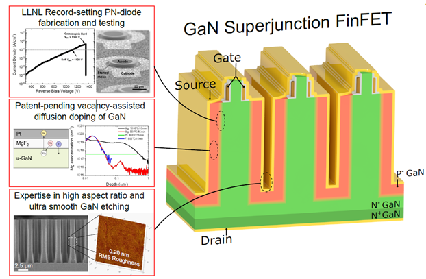
P-type doping of gallium nitride (GaN) enabled the proliferation of light emitting diodes and laser diodes based on III-Nitride elements (GaN, indium nitride, aluminum nitride, and alloys thereof). It is also useful in high power electronics, such as diodes and transistors. The problem that the industry faced is the theoretical limit of silicon in power semiconductors. The superjunction concept has played a fundamental role in overcoming this limit. This invention provides a novel method in creating superjunction devices.
The approach is to use Charge Balance Layers (CBLs) to create a superjunction device in wide bandgap materials. These CBLs enable the device to effectively spread the electric field over 2- or 3-dimensions within a semiconductor voltage sustaining layer instead of 1-dimension, thereby increasing the maximum voltage a device is capable of withstanding. The challenge of using CBLs is the difficulty of complex dopant patterning. LLNL has filed a U.S. Patent (Application No. 17/166,962 Field Assisted Interfacial Diffusion Doping Through Heterostructure Design) which describes a simpler solution compared to MOCVD or ion implantation. In addition, by measuring the film impedance or optical properties during diffusion, a feedback mechanism can be established such that tight control of the resulting doping profile can be monitored.
The novelty is the use of field-assisted diffusion of dopants to create the CBLs needed for a superjunction device.
N. P. Allen, Gallium Nitride Superjunction Transistor: Continued Funding Report LLNL-TR-840432, September 28, 2022 (https://www.osti.gov/servlets/purl/1890078)
L. F. Voss, et al., 2021. "Prospects for Magnesium diffusion doping of GaN." Electrochemical Society. LLNL-ABS-821793 (https://doi.org/10.1149/MA2021-0234999mtgabs).
Noah Allen, Gallium Nitride Superjunction Fin Field Effect Transistor 21-ERD-036, LLNL-TR-827723, October 18, 2021 (https://www.osti.gov/servlets/purl/1826468)
- Reduced manufacturing cost of superjunction devices.
- Can use commercially available semiconductor manufacturing equipment
- Controllable doping profile during deposition
- High power electronics
- LEDs and Laser Diodes
Current stage of technology development: TRL 2 (Technology concept and application formulated)
U.S. Patent No. 10,930,506 Gallidation Assisted Impurity Doping issued 2/23/2021 (https://image-ppubs.uspto.gov/dirsearch-public/print/downloadPdf/10930506)
U.S. Patent Application No. 2021/0257463 Field Assisted Interfacial Diffusion Doping Through Heterostructure Design published 8/19/2021 (https://image-ppubs.uspto.gov/dirsearch-public/print/downloadPdf/20210257463)
U.S. Patent Application No. 17/880,552 Superjunction Devices Formed by Field Assisted Diffusion of Dopants