
This portfolio was organized to group innovations that might not be categorized in the other portfolios. Instruments are full systems integrated to perform complex electrical or mechanical work. Sensors are devices that detect, measure, or locate a physical property. Electronics are devices that manipulate electrons or control electrical energy, and the manufacturing processes that fabricate them.
Portfolio News and Multimedia
The trade journal R&D World Magazine recently announced the winners of the awards, often called the “Oscars of innovation,” recognizing new commercial products, technologies and materials that are available for sale or license for their technological significance.
Lawrence Livermore National Laboratory (LLNL) scientists and engineers have earned four awards among the top 100 inventions worldwide. With this year’s results, the Laboratory has now collected a total of 186 R&D 100 awards since 1978.
Submitted through LLNL’s Innovation and Partnerships Office (IPO), these awards recognize the impact that Livermore innovation, in collaboration with industry partners, can have on the U.S. economy as well as globally.
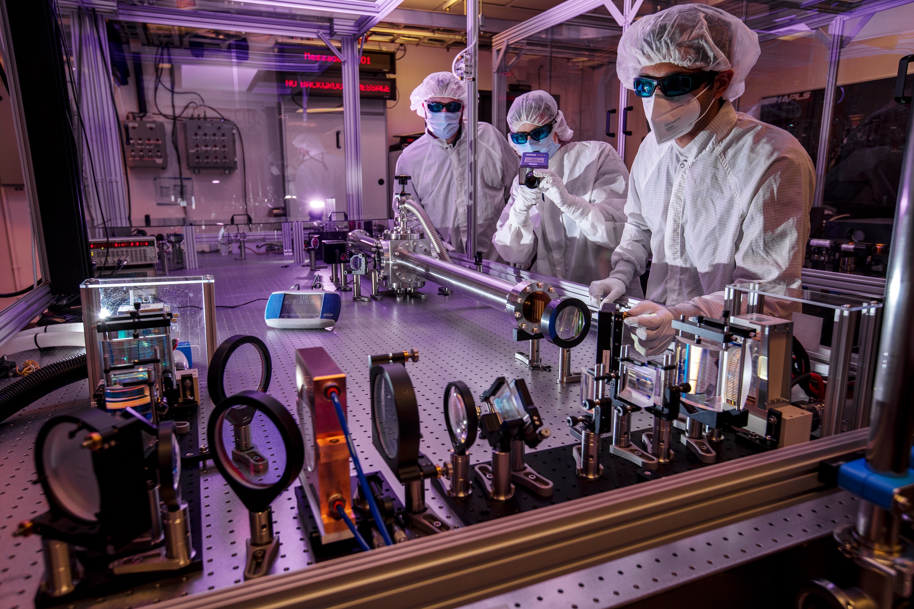
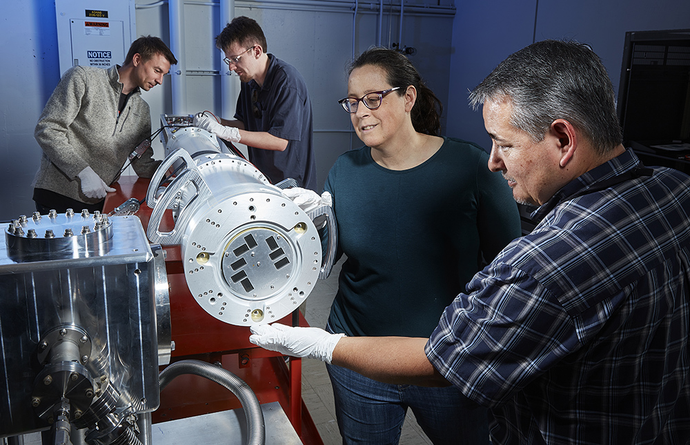
Decades of cutting-edge laser, optics and plasma physics research at Lawrence Livermore National Laboratory (LLNL) played a key role in the underlying science that the semiconductor industry uses to manufacture advanced microprocessors. Now a new research partnership led by LLNL aims to lay the groundwork for the next evolution of extreme ultraviolet (EUV) lithography, centered around a Lab-developed driver system dubbed the Big Aperture Thulium (BAT) laser.
LLNL plasma physicists, Brendan Reagan and Jackson Williams, are the project’s co-lead principal investigators. The project includes scientists from SLAC National Accelerator Laboratory; ASML San Diego; and the Advanced Research Center for Nanolithography (ARCNL), a public-private research center based in the Netherlands.
Funded through DOE’s Unlocking Lasting Transformative Resiliency Advances by Faster Actuation of power Semiconductor Technologies (ULTRAFAST) program, LLNL researchers (in Engineering) will develop an optically-controlled semiconductor transistor to enable future grid control systems to accommodate higher voltage and current than state-of-the-art devices. (Award amount: $3,000,000) while LLNL licensee Opcondys will develop a light-controlled grid protection device to suppress destructive, sudden transient surges on the grid such as those caused by lightning and electromagnetic pulses. (Award amount: $3,178,977)
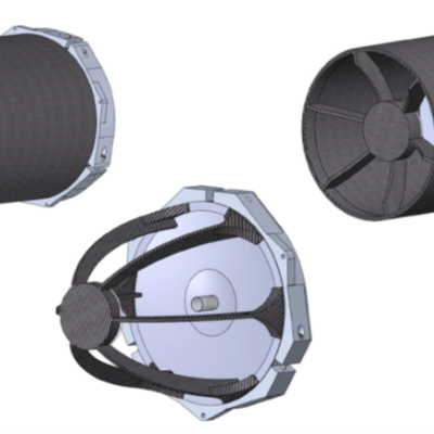
The approach is to use foundational materials science, structural design, thermal analysis, optic fabrication, and space systems engineering, and to use optimize them through large-scale simulation to realize meter-scale telescopes at 10X cost reduction. LLNL’s folded Gregorian design integrates all alignment sensitive components into one static monolithic system. Like solid-…

LLNL developed a novel SOS diode structure starting with a n-type silicon wafer. On the appropriate sides of the wafer, donor and acceptor dopants with specifically designed and optimized concentration profiles are diffused in the structure. Crucially, an extra n-region is introduced to the structure to address pre-pulses. The result is a SOS diode with an optimized p+/p/n-…

LLNL researchers have developed an approach to form silicon carbide (and diamond) nanoneedles using plasma etching that create micro pillars followed by chemical etching of the pillars in forming gas containing hydrogen and nitrogen. Combining these two etching processes allow for fabrication of micro- and nanoneedles that are thinner and sharper than conventionally fabricated needles.

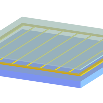
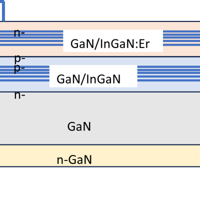
The approach is to use appropriately doped semi-insulating gallium nitride to provide a high damage tolerant photoconductor with high responsivity to various pump wavelength light. Mn, C, or Fe are used as dopants to provide a source of electrons or holes that can be excited. This is combined with the use of dichroic antireflection coating at the GaN/polyimide/liquid crystal…

This LLNL invention introduces a technique for optimally detuning the ADC and signal clocks while maintaining synchronization between the two to manage correlated errors in waveform processing. This technique maintains synchronization between the two clocks, but with optimal detuning applied the interleaving artifacts are maximally decorrelated across waveforms and thus suppressed with…
LLNL researchers have developed a relatively large electrochemically active window with low sheet resistance yet has dramatically increased RF transmission. In-situ measurements show an ~40% increase in reflection at 12GHz when tinting for 10 minutes as compared to the off state. The researchers achieved this through combining novel geometric design of the metal traces with the…
This LLNL invention is a wide bandgap (WBG) or ultra-wide bandgap (UWBG) material comprising a PCSS that is modified, either chemically through alloying and/or mechanically through strain fields, in order to tune the energetic positions of the valence and/or conduction bands and the associated optical transition energies that create and quench the PCSS responsivity.
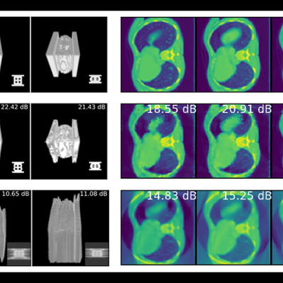
LLNL’s Distributed Implicit Neural Representation (DINR) is a novel approach to 4D time-space reconstruction of dynamic objects. DINR is the first technology to enable 4D imaging of dynamic objects at sufficiently high spatial and temporal resolutions that are necessary for real world medical and industrial applications.

LLNL researchers have developed a TDLAS-based, standalone, real-time gas analyzer in a small form-factor for continuous or single-point monitoring. The system can analyze multiple gases with ultra-high sensitivity (ppm detection levels) in harsh conditions when utilizing wavelength-modulation spectroscopy (WMS).
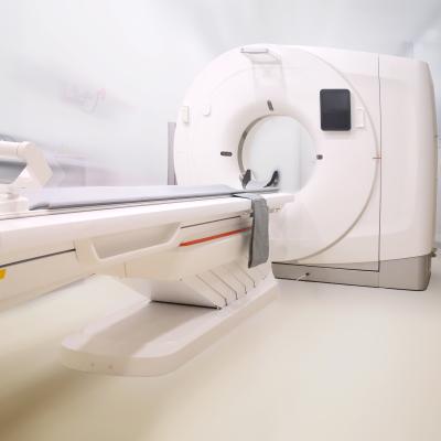
The essence of this invention is a method that couples network architecture using neural implicit representations coupled with a novel parametric motion field to perform limited angle 4D-CT reconstruction of deforming scenes.

A thyristor will stay conducting until the current through the device is zero (“current zero”) or perhaps slightly negative. LLNL’s approach is to use the opticondistor (“OTV”) to force this current zero in order to force the device into an “off” state. By combining a light-activated thyristor with an OTV, a noise-immune, high efficiency, high-power switching device can be…

The researchers’ approach leverages the concept that dopants have high diffusivities in Ga2O3; the key lies in the selection of the appropriate dopant. This LLNL invention describes two device types that employ this design:

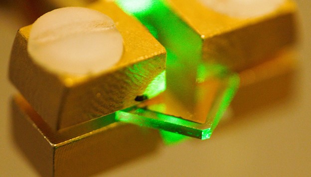
Design and construction of a photoconductive switch requires a diamond photoconductor illuminated by light of a certain excitation wavelength.
Characteristics of the LLNL-developed switch are as follows:

LLNL researchers has developed designs to augment WBG/UWBG-based OALVs to improve their power handling capability under CW operational environments. These designs include:
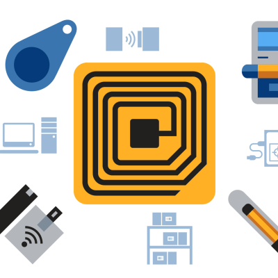
LLNL researchers have developed a novel Radio Frequency Identification (RFID), tracking, powering system and method using coded Ultra-wideband (UWB) signaling. The RFID system is capable of remote powering (activating) multiple passive UWB tags that are located some distance away, which is further than conventional RFID tags. Once the tags are activated, the tags are able to communicate with…

LLNL researchers have invented an ultrafast PCSS to drive a high-power laser diode with arbitrary pulse widths. These devices operate by supplying a high voltage (>10 kV) to one side of the switch. A short pulse of light illuminates the semiconductor, instantly turning it from highly resistive to highly conductive. Ultrawide bandgap (UWBG) semiconductors are used to achieve sub-…
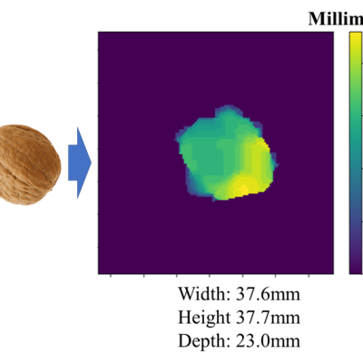
LLNL’s novel technology automates the inspection process by using a scanning system that captures data within the walnut shell without having to open the shell. The system output gives a visual image inside the walnut shell sufficient to evaluate and rate the quality of the walnut. The system uses a camara and radar that can capture data at a rapid rate. This improves speed and…
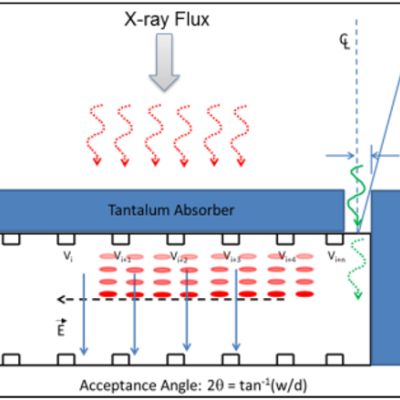
The approach is to develop a solid-state X-ray imager based on the architecture of the Silicon Drift Detector (SDD) which uses a series of cathode strips on both sides of a silicon wafer to achieve bulk depletion and electron drift. The invention leverages this SDD functionality to achieve signal stretching of liberated charge carriers from X-Ray photons that converts the time domain…

The approach is to leverage the fact that a momentary “load” equal to the power transmission line impedance, (Z0), during the transient can suppress its propagation. Z(0) is typically a fixed impedance of several hundred ohms based on the geometry of most single wire transmission lines.
So, an isolated self-powered opticondistor (OTV) system may provide an ultrafast method of…

LLNL’s novel approach is to use diamond substrates with the desired donor (nitrogen) and acceptor (boron) impurities. In order to optically activate these deep impurities, the invention requires at least one externally or internally integrated light source. The initial exposure to light can set up the desired conduction current, after which the light source could be turned…

Instead of producing individual DSRDs and bonding them, Tunnel DSRD's entire stack structure is grown epitaxially on a n- or p-type silicon wafer, resulting in a novel, “monolithic” stacked DSRD. A tunnel diode is essentially a diode with very highly doped p and n regions such that the reverse breakdown voltage is 200 meV or lower.
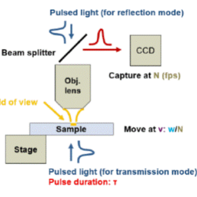
LLNL’s novel approach is to use a continuous moving camera with a scan speed of >1 mm/sec and a frame rate of 100 frames per second. The key is to have a light source that flashes with a duration of one nanosecond, thus essentially freezing the image with no blur. Clear images of high resolution can then be captured through a high-magnification objective lens (reflection mode)…

U.S. Patent No. 11,555,965 describes LLNL’s invention of “Illumination Frustums” for photoconductive switches to capture and “frustrate” the light from leaving the frustum. LLNL researcher’s latest novel invention, “Twister Oven”, achieves this by encouraging laser light absorption in a photo conductor material. Light enters the oven twisting and reflecting, making near normal…

For cooling a high power device, the novel approach is to use a thermoelectric cooler (TEC)-based embedded substrate with proper selection of the TEC material as an active cooler. The packaging configuration of TEC allows cooling the entire die without the use of a fluid. The process is compatible with the thin film TEC material. Standard semiconductor processes can be used…
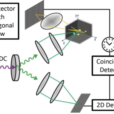
LLNL’s approach to the development of a wide-field, three-dimensional quantum (3DQ) microscope is to harness quantum entangled photons to form simultaneous 3D optical images, which could be a new paradigm for 3D volumetric imaging of biological specimens. The 3DQ microscope is comprised of a novel optical system with highly sensitive detectors and an on-demand light source of entangled…

LLNL researchers faced this challenge by bridging the gap between VEDs and solid-state electronics (SSE). Their approach was to create a hybrid vacuum microelectronic device (VMD) architecture that combines the properties of vacuum as the electronic medium and the compact form factor and manufacturing scalability of semiconductor microelectronic chips.

For this method, a Silicon on Insulator (SOI) wafer is used to tailor etch rates and thickness in initial steps of the process. The simple three step process approach is comprised of grayscale lithography, deep reactive-ion etch (DRIE) and liftoff of the SOI wafer. The liftoff process is used to dissolve the insulating layer, thus separating sections of the wafer as individual…
LLNL’s novel approach combines 2-color spectroscopy with CRDS, a combination not previously utilized.

The approach is to use Charge Balance Layers (CBLs) to create a superjunction device in wide bandgap materials. These CBLs enable the device to effectively spread the electric field over 2- or 3-dimensions within a semiconductor voltage sustaining layer instead of 1-dimension, thereby increasing the maximum voltage a device is capable of withstanding. The challenge of using CBLs is…
The approach is to build a high voltage insulator consisting of two materials: Poly-Ether-Ether-Ketone (“PEEK”) and Machinable Ceramic (“MACOR”). PEEK has a high stress tolerance but cannot withstand high temperatures, while MACOR has high heat tolerance but is difficult to machine and can be brittle. MACOR is used for the plasma-facing surface, while PEEK will handle the…

Design and construction of a photoconductive switch requires a diamond photoconductor illuminated by light of a certain excitation wavelength. The diamond material is specifically doped with substitutional nitrogen, which act as a source of electrons. The device architecture allows maximum light entering the aperture. The top and bottom electrodes are made of ultra wide band…

The approach is to use a custom-designed frustrum and attach it to the optical fiber that connects to the PCSS. Light from the fiber enters the frustrum, spreads out, and enters the PCSS. Any unabsorbed light re-enters the frustrum and, because of its geometry, reflects back into the PCSS itself with only a negligible fraction escaping from the fiber. The shape of the novel…
LLNL has developed a method of extending device lifetimes by imprinting into the device a shape that excludes specific vibrational modes, otherwise known as a phononic bandgap. Eliminating these modes prevents one of the primary energy loss pathways in these devices. LLNL’s new method enhances the coherence of superconducting circuits by introducing a phononic bandgap around the system’s…
To solve these challenges using new and existing CT system designs, LLNL has developed an innovative software package for CT data processing and reconstruction. Livermore Tomography Tools (LTT) is a modern integrated software package that includes all aspects of CT modeling, simulation, reconstruction, and analysis algorithms based on the latest research in the field. LTT contains the most…
LLNL's 3D X-ray imager combines two different hardware pieces. The first is an x-ray optic with a depth-of-field that is small compared to the object under investigation. Reflective Wolter type x-ray optics are one such design. These hollow optics have a relatively large collection efficiency and can be designed with a large field of view. The depth of focus, which is the distance over which a…

LLNL researchers have designed and tested performance characteristics for a multichannel pyrometer that works in the NIR from 1200 to 2000 nm. A single datapoint without averaging can be acquired in 14 microseconds (sampling rate of 70,000/s). In conjunction with a diamond anvil cell, the system still works down to about 830K.
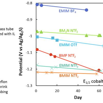
LLNL has developed a reference electrode that is a great improvement on the widely used silver or platinum wire QRE commonly used in electrochemistry in ionic liquids. This new reference electrode, based on a silver-sulfide coated silver wire, exhibits greatly improved stability over a QRE. The stability of our RE approaches that of the Ag/Ag+ RE, but unlike the Ag/Ag+ RE, the RE reported here…
LLNL's method of equivalent time sampling incorporates an embedded system that generates the pulses used to trigger the external circuit and the data acquisition (DAQ). This removes the external reference clock, allowing the overall system clock rate to change based on the ability of the embedded system. The time delays needed to create the time stepping for equivalent time sampling is done by…

LLNL’s Optically-based Interstory Drift Meter System provides a means to accurately measure the dynamic interstory drift of a vibrating building (or other structure) during earthquake shaking. This technology addresses many of the shortcomings associated with traditional strong motion accelerometer based building monitoring.
LLNL’s discrete diode position sensitive device is a newly…
The technology that is available has the capability to inject realistic radiation detection spectra into the amplifier of a radiation detector and produce the all the observables that are available with that radiation detection instrument; count-rate, spectrum, dose rate, etc.
The system uses the capability of LLNL to generate the source output for virtually any source and determine…

The Optical Transconductance Varistor (OTV, formerly Opticondistor) overcomes depletion region voltage limitations by optically exciting wide bandgap materials in a compact package. A 100μm thick crystal could have the capability approaching 40kV and would replace numerous equivalent junction devices. Thus, unlike present junction transistors or diodes, this wide bandgap device can be stacked…
LLNL's high fidelity hydrocode is capable of predicting blast loads and directly coupling those loads to structures to predict a mechanical response. By combining this code and our expertise in modeling blast-structure interaction and damage, along with our access to experimental data and testing facilities, we can contribute to the design of protective equipment that can better mitigate the…