
Silicon carbide has properties that make it ideal for electronic, MEMS and transdermal drug delivery devices (e.g., high thermal conductivity, chemical resistance and biocompatibility). Conventional fabrication of silicon carbide microneedles uses molds typically prepared by using a mixture of resin and hydrate material. This methods limits the shape of the tapered sharp tip. By adapting semiconductor processing methods to this application may allow for nano-level precision. The challenge is that etching processes, particularly isotropic etching, that work well for silicon do not work for silicon carbide since the latter is relatively inert.
LLNL researchers have developed an approach to form silicon carbide (and diamond) nanoneedles using plasma etching that create micro pillars followed by chemical etching of the pillars in forming gas containing hydrogen and nitrogen. Combining these two etching processes allow for fabrication of micro- and nanoneedles that are thinner and sharper than conventionally fabricated needles.
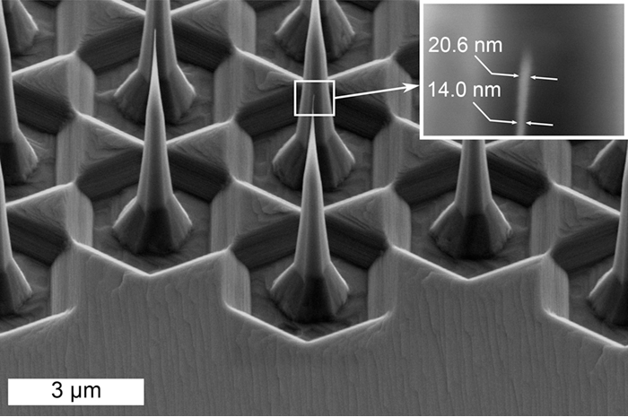
Image Caption: 4H-SiC tips fabricated by etching 2 μm wide pillars at 1550 °C for 1 h. The inset shows that the tips are as narrow as 15 nm in diameter.
Fabrication of micro and nanoneedles with tips as narrow as 15 nm that cannot be fabricated using conventional fabrication methods (e.g., from molds made of resin and hydrate material).
- Optical switches
- Field emission tips
- Probes for atomic force microscopes
- Transdermal delivery of drugs and proteins
- Electronic applications
- Diamond nanoneedles
Current stage of technology development: TRL ☐ 0-2 ☒ 3-5 ☐ 5-9
LLNL has filed for patent protection on this invention.
U.S. Patent Application No. 12246155 SILICON CARBIDE NANONEEDLES AND FABRICATION THEREOF published 3/11/2025