

LLNL developed a novel SOS diode structure starting with a n-type silicon wafer. On the appropriate sides of the wafer, donor and acceptor dopants with specifically designed and optimized concentration profiles are diffused in the structure. Crucially, an extra n-region is introduced to the structure to address pre-pulses. The result is a SOS diode with an optimized p+/p/n-…
Image
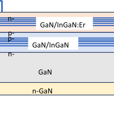
This LLNL invention is a wide bandgap (WBG) or ultra-wide bandgap (UWBG) material comprising a PCSS that is modified, either chemically through alloying and/or mechanically through strain fields, in order to tune the energetic positions of the valence and/or conduction bands and the associated optical transition energies that create and quench the PCSS responsivity.
Image

Instead of producing individual DSRDs and bonding them, Tunnel DSRD's entire stack structure is grown epitaxially on a n- or p-type silicon wafer, resulting in a novel, “monolithic” stacked DSRD. A tunnel diode is essentially a diode with very highly doped p and n regions such that the reverse breakdown voltage is 200 meV or lower.
Image

For cooling a high power device, the novel approach is to use a thermoelectric cooler (TEC)-based embedded substrate with proper selection of the TEC material as an active cooler. The packaging configuration of TEC allows cooling the entire die without the use of a fluid. The process is compatible with the thin film TEC material. Standard semiconductor processes can be used…
Image

LLNL researchers faced this challenge by bridging the gap between VEDs and solid-state electronics (SSE). Their approach was to create a hybrid vacuum microelectronic device (VMD) architecture that combines the properties of vacuum as the electronic medium and the compact form factor and manufacturing scalability of semiconductor microelectronic chips.
Image

The approach is to use Charge Balance Layers (CBLs) to create a superjunction device in wide bandgap materials. These CBLs enable the device to effectively spread the electric field over 2- or 3-dimensions within a semiconductor voltage sustaining layer instead of 1-dimension, thereby increasing the maximum voltage a device is capable of withstanding. The challenge of using CBLs is…
Image
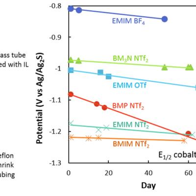
LLNL has developed a reference electrode that is a great improvement on the widely used silver or platinum wire QRE commonly used in electrochemistry in ionic liquids. This new reference electrode, based on a silver-sulfide coated silver wire, exhibits greatly improved stability over a QRE. The stability of our RE approaches that of the Ag/Ag+ RE, but unlike the Ag/Ag+ RE, the RE reported here…
Image

The Optical Transconductance Varistor (OTV, formerly Opticondistor) overcomes depletion region voltage limitations by optically exciting wide bandgap materials in a compact package. A 100μm thick crystal could have the capability approaching 40kV and would replace numerous equivalent junction devices. Thus, unlike present junction transistors or diodes, this wide bandgap device can be stacked…