Image
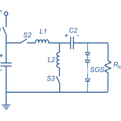
Schematic of the SOS switching circuit

LLNL developed a novel SOS diode structure starting with a n-type silicon wafer.  On the appropriate sides of the wafer, donor and acceptor dopants with specifically designed and optimized concentration profiles are diffused in the structure.  Crucially, an extra n-region is introduced to the structure to address pre-pulses.  The result is a SOS diode with an optimized p+/p/n-…

Image
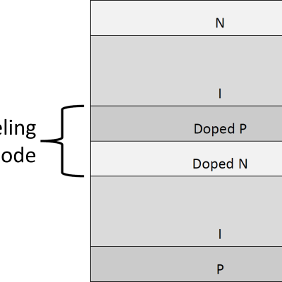
Tunneling Diode between two DSRDs

Instead of producing individual DSRDs and bonding them, Tunnel DSRD's entire stack structure is grown epitaxially on a n- or p-type silicon wafer, resulting in a novel, “monolithic” stacked DSRD.  A tunnel diode is essentially a diode with very highly doped p and n regions such that the reverse breakdown voltage is 200 meV or lower.