
Although silicon still constitutes 95% of the device types available in the market, heat management continues to challenge its use in power electronics. Diamond, an ultrawide bandgap (UWBG) material, can run hotter than silicon without a degradation in performance, can more easily be cooled, can tolerate higher voltages before failure, and electrons can move faster through the material. Because of these characteristics, diamond is superior to other UWBG materials like SiC, GaN, GaO, and AlN. Diamond-based semiconductors are capable of increasing power density as well as creating faster lighter, and simpler devices.
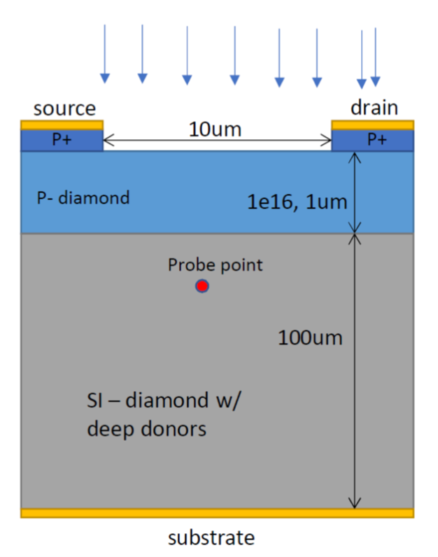
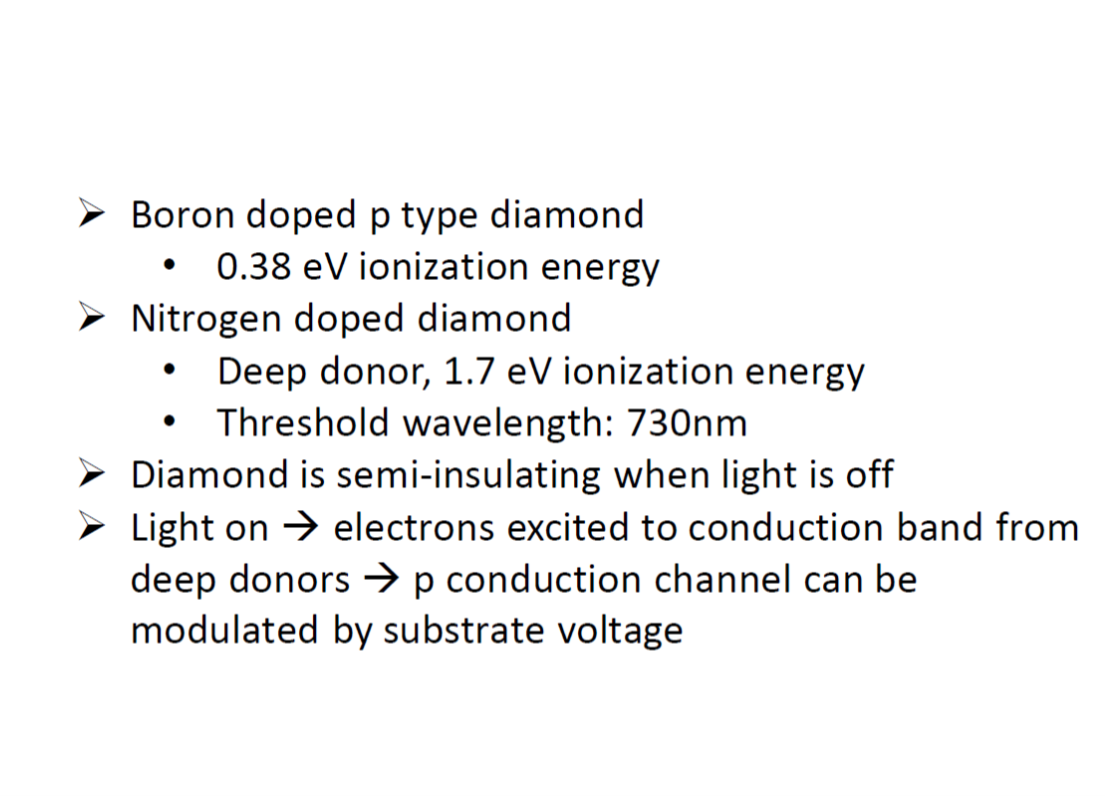
LLNL’s novel approach is to use diamond substrates with the desired donor (nitrogen) and acceptor (boron) impurities. In order to optically activate these deep impurities, the invention requires at least one externally or internally integrated light source. The initial exposure to light can set up the desired conduction current, after which the light source could be turned off. Even with the light turned off, the device can still maintain the desired current condition, and the electric current remains conducting. The device is a planar design, but it can be improved upon by adding Fin and OGAA structures. Additionally, an optical junction termination extension (O-JTE) used to suppress the high electric field that appears at the vicinity of the corners between gate and p-channel.
- Value Proposition: Less operating costs relative to other photoconductive switches.
- The switch is non-volatile, meaning it retains its status for a long time without the need of sustaining electric or optical power.
- Power Electronics
- Applications needing high voltage switches
Current stage of technology development: TRL 2
LLNL has filed for patent protection on this invention.