
Ongoing miniaturization, the manufacturing of ever-smaller products and devices, has led LLNL researchers to explore the many ways to microfabricate objects with features in the micron scale in larger quantities. Common microfabrication processes, particularly for complex geometries have a number of drawbacks. Depending on the process, the limitations range from not achieving the desired shape, being slow/have low throughput to requiring multiple steps and higher-level expertise. There is a need for a more reliable and efficient method to produce complex 3D silicon micro-objects of customizable shape in less steps than what is currently available.
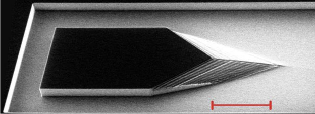
LLNL’s novel method of producing silicon microstructures was spurred by research to fabricate neural implant stiffeners that are to be used for chronic implantation of electrode arrays in the brain for monitoring its activity. The fabrication of these devices are time-consuming due to the complexity of the 3D shanks, which are designed to reduce insertion force. LLNL researchers have developed a simple three step process comprised of commonly available fabrication procedures to allow for a faster microfabrication process for such stiffeners as well as other similar objects.
For this method, a Silicon on Insulator (SOI) wafer is used to tailor etch rates and thickness in initial steps of the process. The simple three step process approach is comprised of grayscale lithography, deep reactive-ion etch (DRIE) and liftoff of the SOI wafer. The liftoff process is used to dissolve the insulating layer, thus separating sections of the wafer as individual silicon objects. This approach allows for production of these objects to be performed in far fewer steps than it would otherwise take if attempted by other more common means.
J. Gleick, A. Yorita, R. Haque “Fabrication of 3-Dimensional Silicon Structures with Greyscale DRIE”, 2021 43rd Annual International Conference of the IEEE Engineering in Medicine & Biology Society (EMBC) Oct 31 - Nov 4, 2021. (https://paperhost.org/proceedings/embs/EMBC21/files/2386.pdf)
- Much greater efficient process with fewer steps resulting in reduced cost and time savings
- Higher throughput (wafer-scale)
- Applicable to any need for solid silicon microstructures
Fabrication of 3D silicon microstructures for objects such as:
- Surgical shuttles for use with implantable devices (e.g. neural implant stiffeners)
- MEMS components
- Silicon lenses (e.g. Fresnel lenses)
Current stage of technology development: TRL 2 (Technology concept and/or application formulated)
US Patent Application Publication No. 2023/0025444 SYSTEMS AND METHODS FOR SILICON MICROSTRUCTURES FABRICATED VIA GREYSCALE DRIE WITH SOI RELEASE published 1/26/2023 (https://image-ppubs.uspto.gov/dirsearch-public/print/downloadPdf/20230025444)