
Beta-gallium oxide (b-Ga2O3) is an emerging ultrawide bandgap (UWBG) semiconductor that possesses outstanding physical properties for power electronics and optoelectronics. A challenge for this material is modifying it such that deep level states in the bandgap could be formed. By selecting the appropriate dopant, with both donors and transition metals (TM), b-Ga2O3 would then be a promising photoconductive material for both photoconductive semiconductor switches (PCSS) and optically addressable light valves (OALV). Currently, TM-doped layers would need to be grown by either epitaxy method, which is expensive or thinning bulk material, which produce fragile layers that are hard to process. LLNL researchers were able to develop diffused β-Ga2O3 photoconductive devices without needing to resort to either method and use commercially available b-Ga2O3 material.
The researchers’ approach leverages the concept that dopants have high diffusivities in Ga2O3; the key lies in the selection of the appropriate dopant. This LLNL invention describes two device types that employ this design:
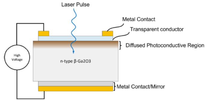
- PCSS: The device consists of an n-type β-Ga2O3 wafer where the top surface is diffused with TM to form a photoconductive layer. A transparent conductor is then deposited onto this photoconductive layer. An ohmic metal contact is placed on the transparent conductor to facilitate electrical interfacing with the switch. On the opposite side of the substrate, a metal contact is placed in contact with the n-type β-Ga2O3 to form both an ohmic contact and act as a mirror.
OALV: The device consists of two wafers/optics that are bonded together to form a liquid crystal cell. The key innovation over other OALV designs is the replacement of bismuth silicon oxide with the diffused β-Ga2O3 photoconductive layer.
Image Caption: A cross-sectional schematic of a diffused b-Ga2O3 photoconductive semiconductor switch (PCSS)
The Value Proposition is Improved performance at less manufacturing costs.
LLNL’s diffused β-Ga2O3 photoconductive devices have numerous advantages over traditional optical switches, such as:
- Outstanding breakdown field strength
- Tunable for optimal device performance.
- Less expensive and easier to manufacture than crystal growth equipment
- High power microwave sources
- High frequency amplifiers and pulse generators
- OALVs
Current stage of technology development: TRL 3
LLNL has filed for patent protection on this invention.
LLNL has a huge portfolio of UWBG-based photoconductive semiconductor switches and OALVs.