LLNL has been at the forefront in developing two-photon polymerization (TPP) additive manufacturing (AM) method. In 2018, LLNL was a recipient of a Federal Laboratory Consortium (FLC) award for their development of FemtoProWrite, which leverages TPP. TPP is a laser light-directed writing technique in which crosslinking reactions initiated by light lead to a change from liquid to solid within a region that is smaller than the light spot. The method is very high resolution, capable of fabricating micro- and nano-scale features.
However, conventional TPP AM printers have extremely slow printing speeds with limited part size since they utilize a single laser spot approach where the laser is directed through a conventional microscope objective and the 3D printed part is built by scanning within the resin material. There is a market need to maintain the high sub-micron printing resolution offered by TPP, while increasing the throughput and dimensions of the printed components.
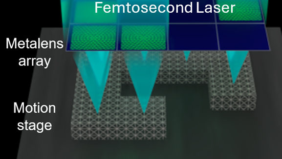
LLNL researchers have developed a parallelized TPP system that combines metalens array and spatial light modulator (SLM) to manipulate the directed laser light, which enables high-volume fabrication of nano-architected structures at wafer-scale. Instead of using a single microscope objective, LLNL’s approach uses an array of metalens that the laser passes through with each metalens being independently controlled via a SLM. This parallelization of printing allows for large scale, high throughput writing of periodic and non-repeating patterns that exceed the capabilities of conventional TPP platforms. This novel approach significantly increases throughput without sacrificing resolution or introducing stitching errors.
Image Caption: Metalens Array used for massively parallel Two-Photon Polymerization (TPP)
- 1000X speed compared to currently available TPP printers
- Wafer-scale
- 100 nm-resolution
- Free of stitching defects
Using the fine resolution of submicron AM, the technology can be used in a wide variety of fields to fabricate functional micro- and nanoscale 3D structures for photonic crystals, micro-optics, mechanical metamaterials, micro fluidics, miniaturized optics, flexible micro-electronics, Micro-electromechanical Systems (MEMS), on-demand 3D chip packaging solutions, custom micro-heatsinks for the next-generation semiconductor and high-density 3D optical memory. TPP can also be used to produce architected materials for energy solutions (e.g., battery and CO2 electrolyzer electrodes) and biomedical engineering (e.g., neural probes).
Current stage of technology development:
TRL ☐ 0-2 ☒ 3-5 ☐ 5-9
LLNL has filed for patent protection on this invention.
U.S. Patent Application No. 2022/0252761System and method for parallel two-photon lithography using a metalens array published 8/11/2022
Download One-Pager


