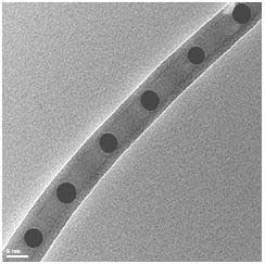
LLNL has patented a process for synthesizing insulating nanowires with regularly-spaced metallic nanospheres, starting from a nanostructured substrate. This technology presents an opportunity for making advanced information storage or processing devices, and for making powerful molecular sensing substrates.
Presently digital data storage is performed with magnetically- or optically-active microstructures or electronically in, for example, a flash memory (e.g., floating gate transistors). A limitation in all these technologies is the planar density with which data elements can be fabricated. LLNL's new technology may allow a very high density of electrically independent nodes to be formed without lithography, thereby increasing the effective data storage density. LLNL's process for synthesizing the nanowires may allow precise placement of the charge-storing structures to facilitate formation of an addressable matrix for both data storage and information processing.
Surface-enhanced Raman effects have been shown to be a powerful tool for selectively enhancing optical signals from target molecules. Micro- and nanostructured substrates have are effective at producing conditions under which enhanced Raman signals can be observed, but these are often defined with expensive lithographic techniques. Because of the high density of metallic nanospheres in the insulating nanowires formed by LLNL's process, these structures may be very useful as Raman-enhancing substrates. A significant advantage of the structures is that they can be created by self-assembly in air with very little processing (and no lithography) required.
The nanosphere synthesis process works when a nanostructured substrate is heated above a critical temperature in the presence of a small amount of metal on the nanostructured surface. The metal acts as a particular type of catalyst for nanowire formation. It is periodically segregated within the nanowire in a thermodynamically well-defined process as nanowires grow. The result is periodically-spaced metal nanoparticles within an insulating nanowire. Dense arrays of nanowires can be formed in this way without lithography of any kind.
|
Feature |
Benefit |
|---|---|
| Density of nanowires on a nanostructured substrate | Improved data storage density; enhanced optical signals for molecular sensing with surface enhanced Raman methods |
| Ease of fabrication (no lithography required) | Reduced fabrication costs for data storage or information processing devices or for molecular sensing substrates |
| Particle-particle proximity within nanowires | Enhanced optical signals for molecular sensing with surface enhanced Raman techniques |
This technology could be used in information storage, data processing or molecular sensing applications. Microelectronics and biotechnology industries can benefit from the advantages presented by LLNL's patented synthesis process.
This technology is at a very early stage of development. An analytical model has been developed to explain the synthesis process, but few experiments have been performed to demonstrate its potential. The synthesis process has been experimentally demonstrated and patented.

