
Powder atomic layer deposition process is used to coat nanopowders of host materials (e.g. yttrium aluminum garnet) with optically active neodymium organometal precursor followed by O2/O3 RF plasma to convert to a single layer of Nd2O3. The process can be repeated to build arbitrarily thick layers with custom doping profiles and followed by post-…
Image
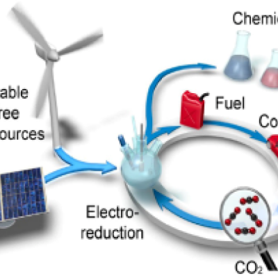
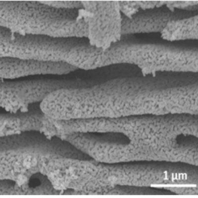
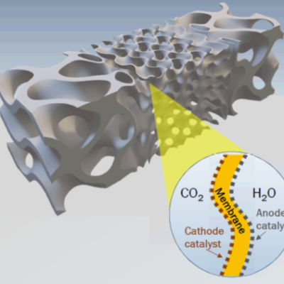
LLNL’s researchers use physical vapor deposition (sputter deposition or electron beam deposition) to coat an inert gasket material (i.e. PTFE) with a conductive metal (i.e. copper). The gas diffusion electrode overlaps onto the copper coated gasket to allow for electrical conductivity between the catalyst surface and the flow field/current collector of a CO2 electrolyzer. The coated gasket…
Image
Using their computational design optimization, LLNL researchers have developed copper-based dilute alloy catalysts (contains <10 at.% of the minority metal alloy component) and demonstrated these novel catalysts have improved energy efficiency and selectivity of the methane conversion reaction. By alloying copper with a small amount of the electropositive minority metal element, the…
Image

This invention proposes using a pulse laser configured to generate laser pulses and a controller for controlling operation of the pulse laser. The controller is further configured to control the pulse laser to cause the pulse laser to generate at least one of the laser pulses with a spatiotemporally varying laser fluence over a duration of at least one of the laser pulses. The spatiotemporally…
Image

This invention proposes to engineer the current density along the length of a laser diode to overcome the penalty associated with non-uniformity resulting from asymmetry in the gain, photon or carrier density despite having uniform contact. Optimizing the current density profile enables diode lasers to operate with greater power conversion efficiency or operate with equivalent power conversion…
Image

This invention proposes to engineer the temperature dependence of the emission wavelength of LEDs and laser diodes. The approach is to use a strain-inducing coating to counteract the intrinsic temperature coefficient of the emission wavelength of the LED or laser diode device thereby rendering it athermal. This invention avoids additional complexity, size, weight and power dissipation of…
Image

This invention proposes a method to overcome the key limitation of electrically pumped lasers based on AlN, AlGaN, or AlInGaN, namely the lack of suitable shallow donor and acceptor dopants. As the band gap of these materials increases (and the emission wavelength decreases), both electrons and holes require greater thermal energies in order to ionize.
Image
Laser diode lensing effect can be substantially reduced by creating a pattern interface such that the substrate is only attached at the diode mesa. This is achieved by either creating a pattern solder joint and/or pattern substrate.
Image

LLNL researchers has developed designs to augment WBG/UWBG-based OALVs to improve their power handling capability under CW operational environments. These designs include:
Image
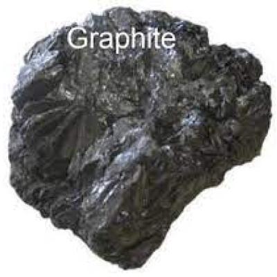
LLNL’s innovation offers an alternate synthetic route to graphite at lower cost using a molten salt mixture of CaCl2-CaCO3-CaO. The synthetic production of graphite and other high-value carbon materials is accomplished in molten salt media via electrochemical reduction and transformation of the carbon from the carbonate ion. The broad electrochemical window of molten salts enables the…
Image

Design and construction of a photoconductive switch requires a diamond photoconductor illuminated by light of a certain excitation wavelength. The diamond material is specifically doped with substitutional nitrogen, which act as a source of electrons. The device architecture allows maximum light entering the aperture. The top and bottom electrodes are made of ultra wide band gap (UWBG)…
Image

The approach is to use a custom-designed frustrum and attach it to the optical fiber that connects to the PCSS. Light from the fiber enters the frustrum, spreads out, and enters the PCSS. Any unabsorbed light re-enters the frustrum and, because of its geometry, reflects back into the PCSS itself with only a negligible fraction escaping from the fiber. The shape of the novel frustrum is…
Image
The novel LLNL approach is to use projection microstereolithography (LAPµSL), starting with a photocurable methacrylate resin formulation consisting of a combination of a photoinitiator, photoabsorber, inhibitor, solvents, and other additives. Prior to use, the resin is pretreated to control viscosity for easier handling. The resin is fed to a LAPµSL printer which employs a near UV light…
Image
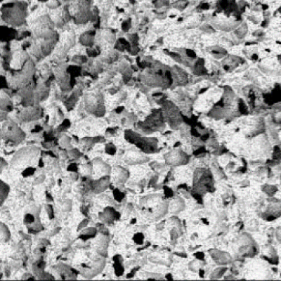
The inventors have developed a 3% Yttria partially-stabilized Zirconia (3YZ) ceramic ink that produces parts with both nano and microporosity and is compatible with two AM techniques: DIW and projection microstereolithography (PμSL). The 3YZ nano-porous ceramic printed parts had engineered macro cavities measuring several millimeters in length, wall thicknesses ranging from 200 to 540 μm, and…
Image
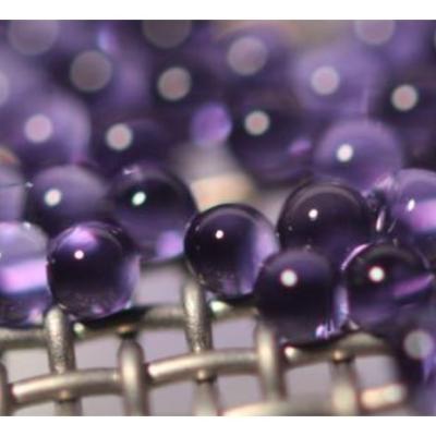
This invention describes a multiple nozzle microfluidic unit that allows simultaneous generation streams of multiple layered coaxial liquid jets. Liquids are pumped into the device at a combined flow rate from 100 mL/hr to 10 L/hr. Droplets are created with diameters in the range of 1 µm to 5 mm and can be created with 1-2 shell layers encapsulating fluid. Droplets created from the system can…
Image

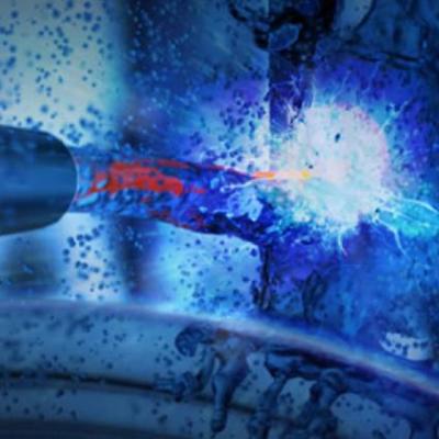
Livermore Lab researchers have developed two new methods for improving the efficiency of laser drilling. The first method is based on multi-pulse laser technology. Two synchronized free-running laser pulses from a tandem-head Nd:YAG laser and a gated CW laser are capable of drilling through 1/8-in-thick stainless-steel targets at a standoff distance of 1 m without gas-assist. The combination of a…
Image
LLNL’s system consists of one or more flashlamp-pumped Nd:glass zig-zag amplifiers, a very low threshold stimulated-Brillouin-scattering (SBS) phase conjugator system, and a free-running single frequency Nd:YLF master oscillator.
Image

The new LLNL technique works by transiently removing and trapping concrete or rock surface material, so that contaminants are confined in a manner that is easy to isolate and remove. Our studies suggest that 10 m2 of surface could be processed per hour. The technique easily scales to more surface/hr.
Image

The Optical Transconductance Varistor (OTV, formerly Opticondistor) overcomes depletion region voltage limitations by optically exciting wide bandgap materials in a compact package. A 100μm thick crystal could have the capability approaching 40kV and would replace numerous equivalent junction devices. Thus, unlike present junction transistors or diodes, this wide bandgap device can be stacked…