

The approach is to use appropriately doped semi-insulating gallium nitride to provide a high damage tolerant photoconductor with high responsivity to various pump wavelength light. Mn, C, or Fe are used as dopants to provide a source of electrons or holes that can be excited. This is combined with the use of dichroic antireflection coating at the GaN/polyimide/liquid crystal…
Image
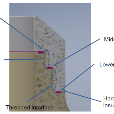
The approach is to build a high voltage insulator consisting of two materials: Poly-Ether-Ether-Ketone (“PEEK”) and Machinable Ceramic (“MACOR”). PEEK has a high stress tolerance but cannot withstand high temperatures, while MACOR has high heat tolerance but is difficult to machine and can be brittle. MACOR is used for the plasma-facing surface, while PEEK will handle the…
Image

LLNL researchers have designed and tested performance characteristics for a multichannel pyrometer that works in the NIR from 1200 to 2000 nm. A single datapoint without averaging can be acquired in 14 microseconds (sampling rate of 70,000/s). In conjunction with a diamond anvil cell, the system still works down to about 830K.