

Powder atomic layer deposition process is used to coat nanopowders of host materials (e.g. yttrium aluminum garnet) with optically active neodymium organometal precursor followed by O2/O3 RF plasma to convert to a single layer of Nd2O3. The process can be repeated to build arbitrarily thick layers with custom doping profiles and followed by post-…
Image

This invention proposes using a pulse laser configured to generate laser pulses and a controller for controlling operation of the pulse laser. The controller is further configured to control the pulse laser to cause the pulse laser to generate at least one of the laser pulses with a spatiotemporally varying laser fluence over a duration of at least one of the laser pulses. The spatiotemporally…
Image
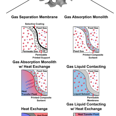
Hierarchical Triply Periodic Minimal Surface Structures For Efficient Two Fluid Flow Reactor Designs
LLNL researchers have devised a set of design principles that facilitates the development of practical TPMS-based two fluid flow reactors.; included in the design are these new concepts:
Image
![Filled (8,8) (left) and (15,15) (right) CNTs with [EMIM+][BF4- ] using SGTI with the proposed spliced soft-core potential (SSCP) approach](/sites/default/files/styles/scale_exact_400x400_/public/2023-10/Filled%20CNTs%20using%20SGTI.png?itok=Dy0ObN7i)
LLNL researchers have developed a novel simulation methodology using slow growth thermodynamic integration (SGTI) utilizing spliced soft-core interaction potential (SSCP). The approach to filling the molecular enclosures is a nonphysical one. Rather than filling the pores from the open ends this method creates steps in the algorithm that allow molecules to pass through the pore…
Image
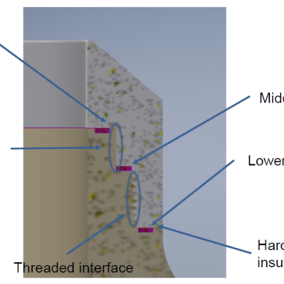
The approach is to build a high voltage insulator consisting of two materials: Poly-Ether-Ether-Ketone (“PEEK”) and Machinable Ceramic (“MACOR”). PEEK has a high stress tolerance but cannot withstand high temperatures, while MACOR has high heat tolerance but is difficult to machine and can be brittle. MACOR is used for the plasma-facing surface, while PEEK will handle the…
Image

Livermore Lab researchers have developed two new methods for improving the efficiency of laser drilling. The first method is based on multi-pulse laser technology. Two synchronized free-running laser pulses from a tandem-head Nd:YAG laser and a gated CW laser are capable of drilling through 1/8-in-thick stainless-steel targets at a standoff distance of 1 m without gas-assist. The combination of a…
Image
By combining 3D printing and dealloying., researchers at LLNL have developed a method for fabricating metal foams with engineered hierarchical architectures consisting of pores at least 3 distinct length scales. LLNL’s method uses direct ink writing (DIW), a 3D printing technique for additive manufacturing to fabricate hierarchical nanoporous metal foams with deterministically controlled 3D…
Image

The new LLNL technique works by transiently removing and trapping concrete or rock surface material, so that contaminants are confined in a manner that is easy to isolate and remove. Our studies suggest that 10 m2 of surface could be processed per hour. The technique easily scales to more surface/hr.
Image

To overcome limitations with cellular silicone foams, LLNL innovators have developed a new 3D energy absorbing material with tailored/engineered bulk-scale properties. The energy absorbing material has 3D patterned architectures specially designed for specific energy absorbing properties. The combination of LLNL's capabilities in advanced modeling and simulation and the additive…