

The approach is to use appropriately doped semi-insulating gallium nitride to provide a high damage tolerant photoconductor with high responsivity to various pump wavelength light. Mn, C, or Fe are used as dopants to provide a source of electrons or holes that can be excited. This is combined with the use of dichroic antireflection coating at the GaN/polyimide/liquid crystal…
Image
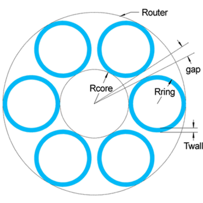
This LLNL invention proposes a new microstructured large mode area fiber design that enhances the confinement of the core mode while strongly suppressing thermal or scattering mediated dynamic couplings with higher order modes thought to be responsible for generating undesirable Transverse Mode Instabilities. The design accomplishes higher order mode suppression and core mode confinement by…
Image

LLNL researchers has developed designs to augment WBG/UWBG-based OALVs to improve their power handling capability under CW operational environments. These designs include:
Image

Design and construction of a photoconductive switch requires a diamond photoconductor illuminated by light of a certain excitation wavelength. The diamond material is specifically doped with substitutional nitrogen, which act as a source of electrons. The device architecture allows maximum light entering the aperture. The top and bottom electrodes are made of ultra wide band…
Image

The approach is to use a custom-designed frustrum and attach it to the optical fiber that connects to the PCSS. Light from the fiber enters the frustrum, spreads out, and enters the PCSS. Any unabsorbed light re-enters the frustrum and, because of its geometry, reflects back into the PCSS itself with only a negligible fraction escaping from the fiber. The shape of the novel…
Image
To replicate the physiology and functionality of tissues and organs, LLNL has developed an in vitro device that contains 3D MEAs made from flexible polymeric probes with multiple electrodes along the body of each probe. At the end of each probe body is a specially designed hinge that allows the probe to transition from lying flat to a more upright position when actuated and then…
Image

Livermore Lab's SBC grating optics benefit from the combination of the following key technologies:
- LLNL proprietary optical coating designs utilizing >100 thin film layers – enables ultra-low-loss, ppm transmission levels through the coating, high diffraction efficiency, and large bandwidth.
- LLNL proprietary dispersive surface relief structure…
Image

The Optical Transconductance Varistor (OTV, formerly Opticondistor) overcomes depletion region voltage limitations by optically exciting wide bandgap materials in a compact package. A 100μm thick crystal could have the capability approaching 40kV and would replace numerous equivalent junction devices. Thus, unlike present junction transistors or diodes, this wide bandgap device can be stacked…