
This invention works by imaging an ultrafast pulse diffracted from a large grating onto a spatial light modulator (SLM) thereby directly transcribing an arbitrary record on a pulse front tilted (PFT) ultrafast pulse. The grating generates PFT of the input pulse, and the SLM provides temporal control of the pulse through the space-to-time mapping of the tilted pulse. Coupling this patterned…
Image

This invention exploits the non-linearities of optical Mach-Zehnder (MZ) electrooptic modulators to enhance small signal dynamic range at higher bandwidths. A linear photodiode (PD) converts the amplified optical signal output from the MZ back to an electrical signal completing an Electrical-Optical-Electrical (EOE) conversion cycle. The dynamic range can be further enhanced by daisy chaining…
Image

This invention proposes to engineer the current density along the length of a laser diode to overcome the penalty associated with non-uniformity resulting from asymmetry in the gain, photon or carrier density despite having uniform contact. Optimizing the current density profile enables diode lasers to operate with greater power conversion efficiency or operate with equivalent power conversion…
Image

This invention proposes to engineer the temperature dependence of the emission wavelength of LEDs and laser diodes. The approach is to use a strain-inducing coating to counteract the intrinsic temperature coefficient of the emission wavelength of the LED or laser diode device thereby rendering it athermal. This invention avoids additional complexity, size, weight and power dissipation of…
Image

This invention proposes a method to overcome the key limitation of electrically pumped lasers based on AlN, AlGaN, or AlInGaN, namely the lack of suitable shallow donor and acceptor dopants. As the band gap of these materials increases (and the emission wavelength decreases), both electrons and holes require greater thermal energies in order to ionize.
Image
Laser diode lensing effect can be substantially reduced by creating a pattern interface such that the substrate is only attached at the diode mesa. This is achieved by either creating a pattern solder joint and/or pattern substrate.
Image
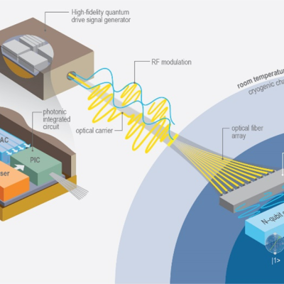
LLNL researchers in the NIF Directorate DoD Technologies RF Photonics Group explored phase modulation solutions to this signal processing challenge. Optical frequency combs offer phase noise characteristics that are orders of magnitude lower than available from commercial microwave references. The Photonics Group researchers recognized that by converting the intensity information into phase,…
Image
To replicate the physiology and functionality of tissues and organs, LLNL has developed an in vitro device that contains 3D MEAs made from flexible polymeric probes with multiple electrodes along the body of each probe. At the end of each probe body is a specially designed hinge that allows the probe to transition from lying flat to a more upright position when actuated and then…