
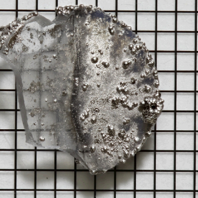
LLNL researchers have continued to develop their pioneering DIW 3D-printed glass optics technology that allows for the 3D printing of single- and multi-material optical glass compositions in complex shapes. This LLNL invention further proposes incorporating dopants (including, but not limited to TiO2 and Pd) into slurries and inks for 3D printing of glass components that can then be directly…
Image

This invention proposes to engineer the current density along the length of a laser diode to overcome the penalty associated with non-uniformity resulting from asymmetry in the gain, photon or carrier density despite having uniform contact. Optimizing the current density profile enables diode lasers to operate with greater power conversion efficiency or operate with equivalent power conversion…
Image

This invention proposes to engineer the temperature dependence of the emission wavelength of LEDs and laser diodes. The approach is to use a strain-inducing coating to counteract the intrinsic temperature coefficient of the emission wavelength of the LED or laser diode device thereby rendering it athermal. This invention avoids additional complexity, size, weight and power dissipation of…
Image

This invention proposes a method to overcome the key limitation of electrically pumped lasers based on AlN, AlGaN, or AlInGaN, namely the lack of suitable shallow donor and acceptor dopants. As the band gap of these materials increases (and the emission wavelength decreases), both electrons and holes require greater thermal energies in order to ionize.
Image
Laser diode lensing effect can be substantially reduced by creating a pattern interface such that the substrate is only attached at the diode mesa. This is achieved by either creating a pattern solder joint and/or pattern substrate.
Image
To replicate the physiology and functionality of tissues and organs, LLNL has developed an in vitro device that contains 3D MEAs made from flexible polymeric probes with multiple electrodes along the body of each probe. At the end of each probe body is a specially designed hinge that allows the probe to transition from lying flat to a more upright position when actuated and then…
Image

LLNL researchers have developed a custom resin formulation which uses a dispersing solvent and only a multifunctional monomer as the binding agent. The dispersing solvent system typically used has multiple components meant to achieve excellent dispersal of silica in order to create a flowable resin (rather than a paste). The dispersing agent has low vapor pressure, which allows the 3D printed…