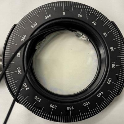
The approach is to use appropriately doped semi-insulating gallium nitride to provide a high damage tolerant photoconductor with high responsivity to various pump wavelength light. Mn, C, or Fe are used as dopants to provide a source of electrons or holes that can be excited. This is combined with the use of dichroic antireflection coating at the GaN/polyimide/liquid crystal…
Keywords
- Show all (240)
- Additive Manufacturing (55)
- Instrumentation (41)
- Synthesis and Processing (21)
- Sensors (14)
- Diagnostics (11)
- Imaging Systems (9)
- Photoconductive Semiconductor Switches (PCSS) (9)
- 3D Printing (8)
- Carbon Utilization (7)
- Electric Grid (7)
- Materials for Energy Products (7)
- Semiconductors (7)
- Substrate Engraved Meta-Surface (SEMS) (7)
- Therapeutics (7)
- Compact Space Telescopes (6)
- Brain Computer Interface (BCI) (5)
- Data Science (5)
- Diode Lasers (5)
- Laser Materials Processing (4)
- (-) Optical Switches (5)
Technology Portfolios

This invention proposes achieving the same effect of a single, high intensity pulse through the use of a closely spaced burst of short duration pulses. By keeping the intensity of the individual pulses below the damage threshold the risk of catastrophic damage is greatly mitigated. Additionally, the pulses are directed to strike the target at locations temporally and spatially sufficiently…
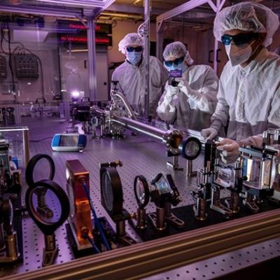
This invention proposes the use of a nonlinear spectral broadening subsystem as a post-CPA pulse compression add-on for high energy laser systems. The proposed solution utilizes the beam profile of a high peak power laser as a reference to shape a highly transmissive nonlinear plastic (e.g., CR39) itself to ensure a spatially homogeneous nonlinear spectral broadening.
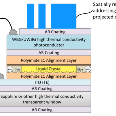
LLNL researchers has developed designs to augment WBG/UWBG-based OALVs to improve their power handling capability under CW operational environments. These designs include:
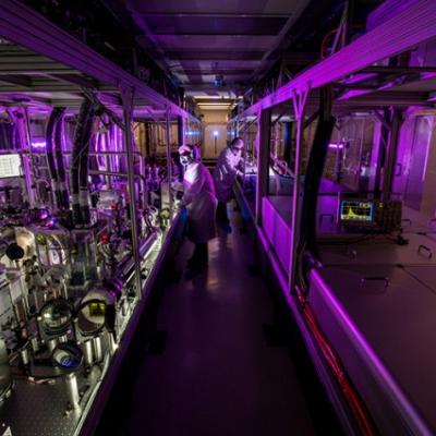
LLNL researchers have developed a high average power Faraday rotator that is gas-cooled and uniquely designed to dissipate heat uniformly so that it does not build up in the optical component and affect its performance. The Faraday rotator material is sliced into smaller disks like a loaf of bread so that high speed helium gas can flow between the slices. With this highly efficient…
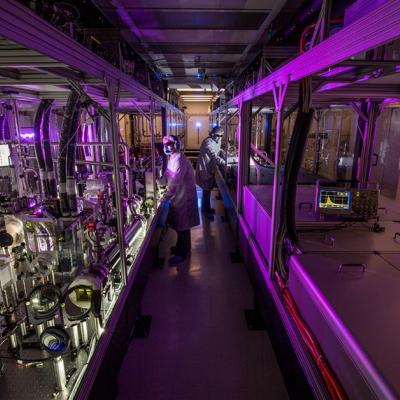
This invention discloses a method to minimize transient variations in the wavelength- and/or pointing-behavior of an optic, without requiring a reduction in its thermal resistance, optical absorption, or operating irradiance. The invention employs a combination of a time-varying heat source and time-varying thermal resistance and/or heat sink temperature to achieve temperature stability of the…
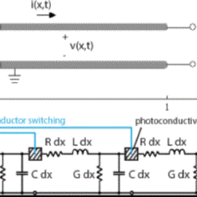
Design and construction of a photoconductive switch requires a diamond photoconductor illuminated by light of a certain excitation wavelength. The diamond material is specifically doped with substitutional nitrogen, which act as a source of electrons. The device architecture allows maximum light entering the aperture. The top and bottom electrodes are made of ultra wide band…
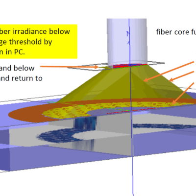
The approach is to use a custom-designed frustrum and attach it to the optical fiber that connects to the PCSS. Light from the fiber enters the frustrum, spreads out, and enters the PCSS. Any unabsorbed light re-enters the frustrum and, because of its geometry, reflects back into the PCSS itself with only a negligible fraction escaping from the fiber. The shape of the novel…
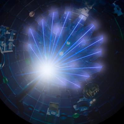
This invention concerns a new type of optic: a transient gas or plasma volume grating produced indirectly by small secondary lasers or directly by nonlinear processes using the primary beams themselves. When used in conjunction with advantageously placed shielding it offers a means of protecting the final optical components of a high-repetition-rate IFE facility. These transmission optics are…
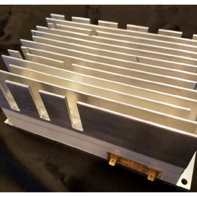
The Optical Transconductance Varistor (OTV, formerly Opticondistor) overcomes depletion region voltage limitations by optically exciting wide bandgap materials in a compact package. A 100μm thick crystal could have the capability approaching 40kV and would replace numerous equivalent junction devices. Thus, unlike present junction transistors or diodes, this wide bandgap device can be stacked…


