
LLNL researchers has developed designs to augment WBG/UWBG-based OALVs to improve their power handling capability under CW operational environments. These designs include:
Image
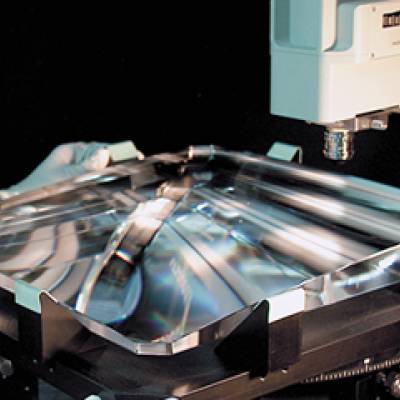
This invention takes advantage of the high water-solubility of key NIF KDP crystal optics and uses water as an etchant to remove surface defects and improve the laser induced damage threshold. Since pure water etches KDP too fast, this invention is to disperse water as nanosized droplets in a water-in-oil micro-emulsion. While in a stable micro-emulsion form, the surfactant additives prevent…
Image
This invention proposes to use laser induced melting/softening to locally reshape the form of a glass optic. The local glass densification that results induces predictable stresses that through plate deformation mechanics yield a deterministic methodology for arbitrarily reshaping an optic surface figure and wavefront without the need to remove material.
Image

Design and construction of a photoconductive switch requires a diamond photoconductor illuminated by light of a certain excitation wavelength. The diamond material is specifically doped with substitutional nitrogen, which act as a source of electrons. The device architecture allows maximum light entering the aperture. The top and bottom electrodes are made of ultra wide band gap (UWBG)…
Image

The approach is to use a custom-designed frustrum and attach it to the optical fiber that connects to the PCSS. Light from the fiber enters the frustrum, spreads out, and enters the PCSS. Any unabsorbed light re-enters the frustrum and, because of its geometry, reflects back into the PCSS itself with only a negligible fraction escaping from the fiber. The shape of the novel frustrum is…
Image

LLNL’s Optically-based Interstory Drift Meter System provides a means to accurately measure the dynamic interstory drift of a vibrating building (or other structure) during earthquake shaking. This technology addresses many of the shortcomings associated with traditional strong motion accelerometer based building monitoring.
LLNL’s discrete diode position sensitive device is a newly…
Image
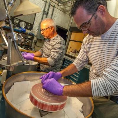
LLNL's Slurry Stabilization Method provides a chemical means of stabilizing a polishing compound in suspension at working concentrations without reducing the rate of material removal. The treated product remains stable for many months in storage.
Image

The Optical Transconductance Varistor (OTV, formerly Opticondistor) overcomes depletion region voltage limitations by optically exciting wide bandgap materials in a compact package. A 100μm thick crystal could have the capability approaching 40kV and would replace numerous equivalent junction devices. Thus, unlike present junction transistors or diodes, this wide bandgap device can be stacked…
Image

The invention relates to a measurement method and system for capturing both the amplitude and phase temporal profile of a transient waveform or a selected number of consecutive waveforms having bandwidths of up to about 10 THz in a single shot or in a high repetition rate mode. The invention consists of an optical preprocessor which can then output a time-scaled replica of the input signal to…