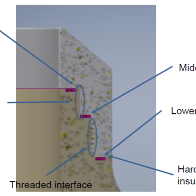
The approach is to build a high voltage insulator consisting of two materials: Poly-Ether-Ether-Ketone (“PEEK”) and Machinable Ceramic (“MACOR”). PEEK has a high stress tolerance but cannot withstand high temperatures, while MACOR has high heat tolerance but is difficult to machine and can be brittle. MACOR is used for the plasma-facing surface, while PEEK will handle the…
Keywords
- (-) Show all (228)
- Additive Manufacturing (51)
- Instrumentation (40)
- Synthesis and Processing (19)
- Sensors (14)
- Diagnostics (12)
- Imaging Systems (9)
- Photoconductive Semiconductor Switches (PCSS) (9)
- 3D Printing (7)
- Electric Grid (7)
- Materials for Energy Products (7)
- Substrate Engraved Meta-Surface (SEMS) (7)
- Therapeutics (7)
- Carbon Utilization (6)
- Semiconductors (6)
- Compact Space Telescopes (5)
- Data Science (5)
- Optical Switches (5)
- Diode Lasers (4)
- Laser Materials Processing (4)
- Precision Optical Finishing (4)
Technology Portfolios
Image

LLNL’s approach is to use their patented Photoconductive Charge Trapping Apparatus (U.S. Patent No. 11,366,401) as the active switch needed to discharge voltage across a vacuum gap in a particle accelerator, like the one described in their other patent (U.S. Patent No.
Image

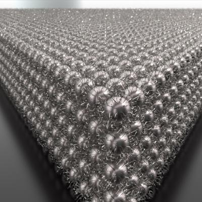
The novel LLNL technique uses electric fields to drive and control assembly. In the literature such methods have heretofore only formed disordered ensembles. This innovative method increases local nanocrystal concentration, initiating nucleation and growth into ordered superlattices. Nanocrystals remain solvated and mobile throughout the process, allowing fast fabrication of ordered…