

The approach is to use appropriately doped semi-insulating gallium nitride to provide a high damage tolerant photoconductor with high responsivity to various pump wavelength light. Mn, C, or Fe are used as dopants to provide a source of electrons or holes that can be excited. This is combined with the use of dichroic antireflection coating at the GaN/polyimide/liquid crystal…
Image

LLNL researchers has developed designs to augment WBG/UWBG-based OALVs to improve their power handling capability under CW operational environments. These designs include:
Image

Design and construction of a photoconductive switch requires a diamond photoconductor illuminated by light of a certain excitation wavelength. The diamond material is specifically doped with substitutional nitrogen, which act as a source of electrons. The device architecture allows maximum light entering the aperture. The top and bottom electrodes are made of ultra wide band…
Image

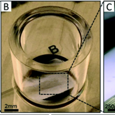
The approach is to use a custom-designed frustrum and attach it to the optical fiber that connects to the PCSS. Light from the fiber enters the frustrum, spreads out, and enters the PCSS. Any unabsorbed light re-enters the frustrum and, because of its geometry, reflects back into the PCSS itself with only a negligible fraction escaping from the fiber. The shape of the novel…
Image
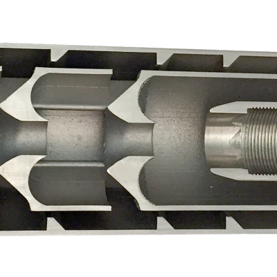
The suppressor has a series of chambers for the propellant to flow through, but unlike all traditional suppressors, the chambers are open, not closed. The propellant is not trapped. It keeps moving. We manage its unimpeded flow through the suppressor. This is the key underlying technology of our suppressor design that enables all the improvements over the 100-year old traditional designs.
Image
To replicate the physiology and functionality of tissues and organs, LLNL has developed an in vitro device that contains 3D MEAs made from flexible polymeric probes with multiple electrodes along the body of each probe. At the end of each probe body is a specially designed hinge that allows the probe to transition from lying flat to a more upright position when actuated and then…
Image
Livermore Lab researchers have developed a tunable shaped charge which comprises a cylindrical liner commonly a metal such as copper or molybdenum but almost any solid material can be used and a surround layer of explosive in which the detonation front is constrained to propagate at an angle with respect to the charge axis. The key to the concept is the ability to deposit a surrounding…
Image
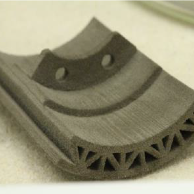
Livermore Lab researchers have developed a method that combines additive manufacturing (AM) with an infill step to render a final component which is energetic. In this case, AM is first used to print a part of the system, and this material can either be inert or energetic on its own. A second material is subsequently added to the structure via a second technique such as casting, melt…
Image

The Optical Transconductance Varistor (OTV, formerly Opticondistor) overcomes depletion region voltage limitations by optically exciting wide bandgap materials in a compact package. A 100μm thick crystal could have the capability approaching 40kV and would replace numerous equivalent junction devices. Thus, unlike present junction transistors or diodes, this wide bandgap device can be stacked…