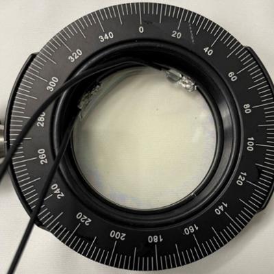
The approach is to use appropriately doped semi-insulating gallium nitride to provide a high damage tolerant photoconductor with high responsivity to various pump wavelength light. Mn, C, or Fe are used as dopants to provide a source of electrons or holes that can be excited. This is combined with the use of dichroic antireflection coating at the GaN/polyimide/liquid crystal…
Keywords
- Show all (240)
- Additive Manufacturing (55)
- Instrumentation (41)
- Synthesis and Processing (21)
- Sensors (14)
- Diagnostics (11)
- Imaging Systems (9)
- Photoconductive Semiconductor Switches (PCSS) (9)
- 3D Printing (8)
- Carbon Utilization (7)
- Electric Grid (7)
- Materials for Energy Products (7)
- Semiconductors (7)
- Substrate Engraved Meta-Surface (SEMS) (7)
- Therapeutics (7)
- Compact Space Telescopes (6)
- Brain Computer Interface (BCI) (5)
- Data Science (5)
- Diode Lasers (5)
- Laser Materials Processing (4)
- (-) Optical Switches (5)
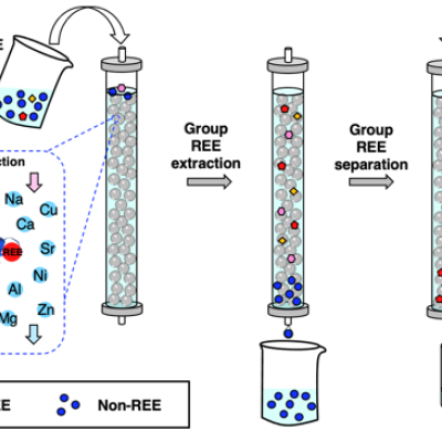
As an important step toward overcoming the technical and environmental limitations of current REE processing methods, the LLNL team has patented and demonstrated a biobased, all-aqueous REE extraction and separation scheme using the REE-selective lanmodulin protein. Lanmodulin can be fixed onto porous support materials using thiol-maleimide chemistry, which can enable tandem REE purification…
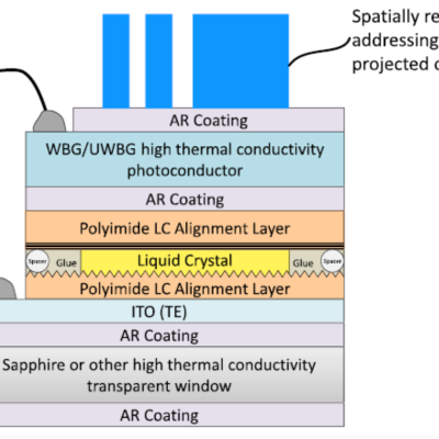
LLNL researchers has developed designs to augment WBG/UWBG-based OALVs to improve their power handling capability under CW operational environments. These designs include:

LLNL researchers have discovered that some inexpensive and commercially available molecules used for other applications, could render certain lanthanide and actinide elements highly fluorescent. These molecules are not sold for applications involving the detection of REEs and actinides via fluorescence. They are instead used as additives in cosmetic products and/or in the pharmaceutical…
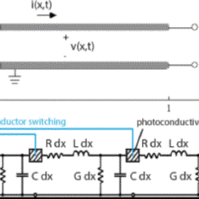
Design and construction of a photoconductive switch requires a diamond photoconductor illuminated by light of a certain excitation wavelength. The diamond material is specifically doped with substitutional nitrogen, which act as a source of electrons. The device architecture allows maximum light entering the aperture. The top and bottom electrodes are made of ultra wide band…
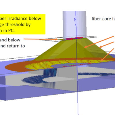
The approach is to use a custom-designed frustrum and attach it to the optical fiber that connects to the PCSS. Light from the fiber enters the frustrum, spreads out, and enters the PCSS. Any unabsorbed light re-enters the frustrum and, because of its geometry, reflects back into the PCSS itself with only a negligible fraction escaping from the fiber. The shape of the novel…
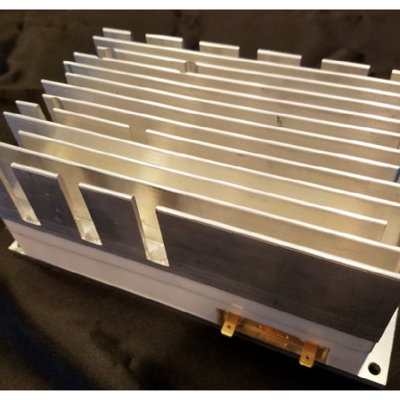
The Optical Transconductance Varistor (OTV, formerly Opticondistor) overcomes depletion region voltage limitations by optically exciting wide bandgap materials in a compact package. A 100μm thick crystal could have the capability approaching 40kV and would replace numerous equivalent junction devices. Thus, unlike present junction transistors or diodes, this wide bandgap device can be stacked…


