Image
4H-SiC tips fabricated by etching 2 μm wide pillars at 1550 °C for 1 h. The inset shows that the tips are as narrow as 15 nm in diameter

LLNL researchers have developed an approach to form silicon carbide (and diamond) nanoneedles using plasma etching that create micro pillars followed by chemical etching of the pillars in forming gas containing hydrogen and nitrogen. Combining these two etching processes allow for fabrication of micro- and nanoneedles that are thinner and sharper than conventionally fabricated needles.

Image
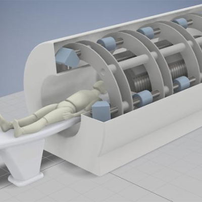
An artist’s concept rendering of a 3.5-meter linear induction accelerator (LIA) with four lines-of-sight toward a patient. The blue elements magnetically focus and direct the LIA’s electron beams.

LLNL’s approach is to use their patented Photoconductive Charge Trapping Apparatus (U.S. Patent No. 11,366,401) as the active switch needed to discharge voltage across a vacuum gap in a particle accelerator, like the one described in their other patent (U.S. Patent No.