
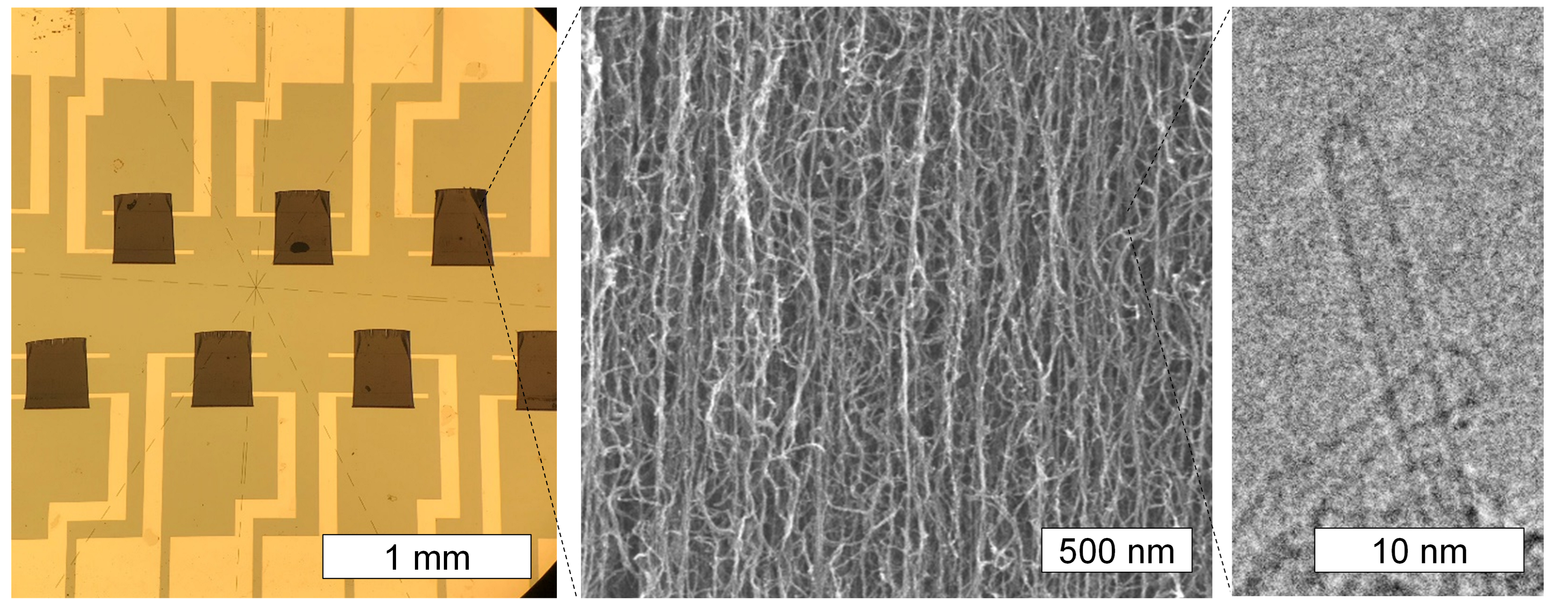
Molecular sensors are important across many industries, including automotive, aerospace, fossil energy, and biomedical (e.g., wearables). Carbon nanotubes (CNTs) have been shown to be particularly promising as molecular sensors because of their high electrical conductivity, thermal and chemical stability, one dimensional form factor, high specific surface area and carbon lattice structure that makes them easy to functionalize. The ability to control and measure the flow of ionic material through CNTs would increase the utility of CNT technologies. This would allow assemblies of nanotubes or other nanostructures to be used as field-effect transistors (FET), electrical sensors, and other devices that rely on electrical current modulation from an externally applied field, or "gate". To maximize sensitivity of a sensing device, it is common to apply a gating voltage to modulate the channel current and maximize the signal gain registered from a detection event. However, gating a thick film comprised of high-surface-area nanostructures or out-of-plane architectures is not possible with typical top-gate and bottom-gate configurations. The electric field may not extend sufficiently or uniformly through the entire ensemble of nanostructures, so their currents will not be modulated as desired.
Existing approaches for gating nanostructured films both non-contact techniques, which involve light probes, as well as contact methods, have limitations. For thick films of nanostructures, light probes are not ideal due to the limits of optical penetration depth. Existing contact methods are not effective for applications where the surface of the nanostructure must remain exposed for functionalization and sensing by direct contact with a medium.
LLNL researchers has devised several design strategies to enable gating of thick architectures (e.g., 2D planar, 3D out-of-plane) made of nanostructures while maintaining substantial surface area available for sensing. Specific examples described in the patent application (2021/0249618) are given for carbon nanotubes (CNTs) and including typical channel gate configurations, gate-all-around strips, gate-all-around in series, core, trench, ridge, or spike gates, and 3D out of plane architectures.
- Can be used in electrical sensors as a means of tuning and maximizing the gain and thus the sensitivity, limit of detection, and response time of the sensor.
- Enables gating of nanostructured films of large thicknesses (> ~100 nm) that extend beyond the electric field generated by typical back-gate or top-gate configurations.
- Leaves a substantial portion of the nanostructure surface exposed so that it can be functionalized and available for sensing in a liquid or gas medium.
- Capable of building out-of-plane architectures to provide gated sensor function with enormous nanostructure surface area on a small footprint.
- Gas and liquid phase molecular sensors
- Field effect transistors for logic gates
Current stage of technology development: TRL 2
LLNL has filed for patent protection on this invention.
U.S. Patent Application No. 2021/0249618 Electrically Gated Nanostructure Devices published 2/8/2021