
Ordered nanocrystal superlattices are emerging materials that have widespread applications in photodetectors, light emitting devices, solid state lasers, solar cells, thermoelectric devices, field effect transistors, and memory devices. The degree of order in the superlattices is crucial for their applications. Currently, nanocrystal superlattices are fabricated with solvent evaporation methods, such as dip coating, spinning coating, spray coating, drop casting, ink jet printing. These processes trade off fabrication speed and crystalline quality of the films; fast fabrication results in disorder or poorly ordered superlattices, whereas a highly ordered superlattice often requires a fairly long fabrication time. Colloidal semiconductor nanocrystals are important building blocks for low-cost, solution-processed electronic devices with tunable functionalities. Thus, a fast and effective method to create nanocrystal films that retains structural ordering is needed.
LLNL researchers have developed two approaches to fabricate nanocrystal superlattices for electronic and optoelectronic devices. Nanocrystals covered by this approach include, but are not limited to, metal nanocrystals, semiconducting nanocrystals (quantum dots), and insulating nanocrystals, or a combination of those.
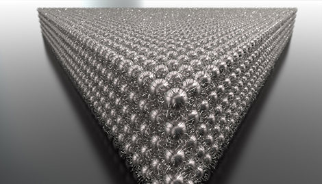
LLNL’s patented approach uses electric fields to drive and control assembly (US Patent No. 11,499,248). This innovative method increases local nanocrystal concentration, initiating nucleation and growth into ordered superlattices. Nanocrystals remain solvated and mobile throughout the process, allowing fast fabrication of ordered superlattices. The fabrication method is faster and offers more tunability than current solvent evaporation or destabilization methods and can produce superlattices with morphologies beyond colloidal crystals in other material systems.
One of the strategies to improving charge transport through nanocrystal films is exchanging of long insulating ligands with shorter passivating ligands. However, it is difficult to retain long-range, close-packed order after the exchange. To address this particular challenge, LLNL researchers have also developed and subsequently filed a patent application (US Patent Application No. 2022/0243352) a novel one-step in situ ligand-exchange method that enables rapid ligand exchange of nanocrystal films that are more than 50 layers thick. The nanocrystal film’s long-range order is retained after ligand exchange from bulky ligand to small organic molecular ligand. Moreover, it is demonstrated that nanocrystal photodetectors made using this method with a well-ordered structure have superior optoelectronic properties compared to disordered films; ordered films have a 16× higher responsivity of ≈0.25 A W−1 at 1 V and a 2× faster response time.
Image Caption: Electric fields assemble silver nanocrystals into a superlattice. Image by Jacob Long/LLNL
Yu Y, Yu D, Orme CA. Reversible, Tunable, Electric-Field Driven Assembly of Silver Nanocrystal Superlattices. Nano Lett. 2017 Jun 14;17(6):3862-3869. https://doi.org/10.1021/acs.nanolett.7b01323
Xu, X., Kweon, K. E., Keuleyan, S., Sawvel, A., Cho, E. J., Orme, C. A., Rapid In Situ Ligand-Exchange Process Used to Prepare 3D PbSe Nanocrystal Superlattice Infrared Photodetectors. Small 2021, 17, 2101166. https://doi.org/10.1002/smll.202101166
LLNL’s patented electric-field driven approach produces highly ordered colloidal crystals in much shorter times and much denser materials than current methods. For example, LLNL researchers have created 2 micron thick films with domain sizes greater than 25 microns and ordered nanoparticle ensembles with a face centered cubic structure that has ~74% of packing density, respectively. This method also allows for tuning the structure of nanoparticle ensembles (e.g., degree of order, lattice constant, degree of preferential orientation, and morphology on patterned surfaces), which is crucial for the fabrication of devices with complex structures. The technique also allows one to change the capping ligands on the surfaces of nanoparticles at the same time as they are being assembled/deposited.
LLNL’s one-step ligand exchange process reduces the time needed for ligand exchange by 2-3 orders of magnitude (from days/several hours to <5 min). This is important for the manufacture of devices for which long-range order or higher density is required to improve performance. The ability to perform rapid ligand exchange on thicker nanocrystal films is of specific interest in many optoelectronic device applications.
- Optoelectronic devices such as photodetectors or quantum dot light emitting diodes (QLEDs)
- Solar cells
- Thermoelectric devices
- Field effect transistors
- Memory devices
Current stage of technology development: TRL 3
LLNL has filed for patent protection on this invention.
US Patent No. 11499248 Electric field driven assembly of ordered nanocrystal superlattices published 11/15/2022
U.S. Patent Application No. 2022/0243352 Ligand Exchange Of Nanocrystal Films published 8/4/2022