
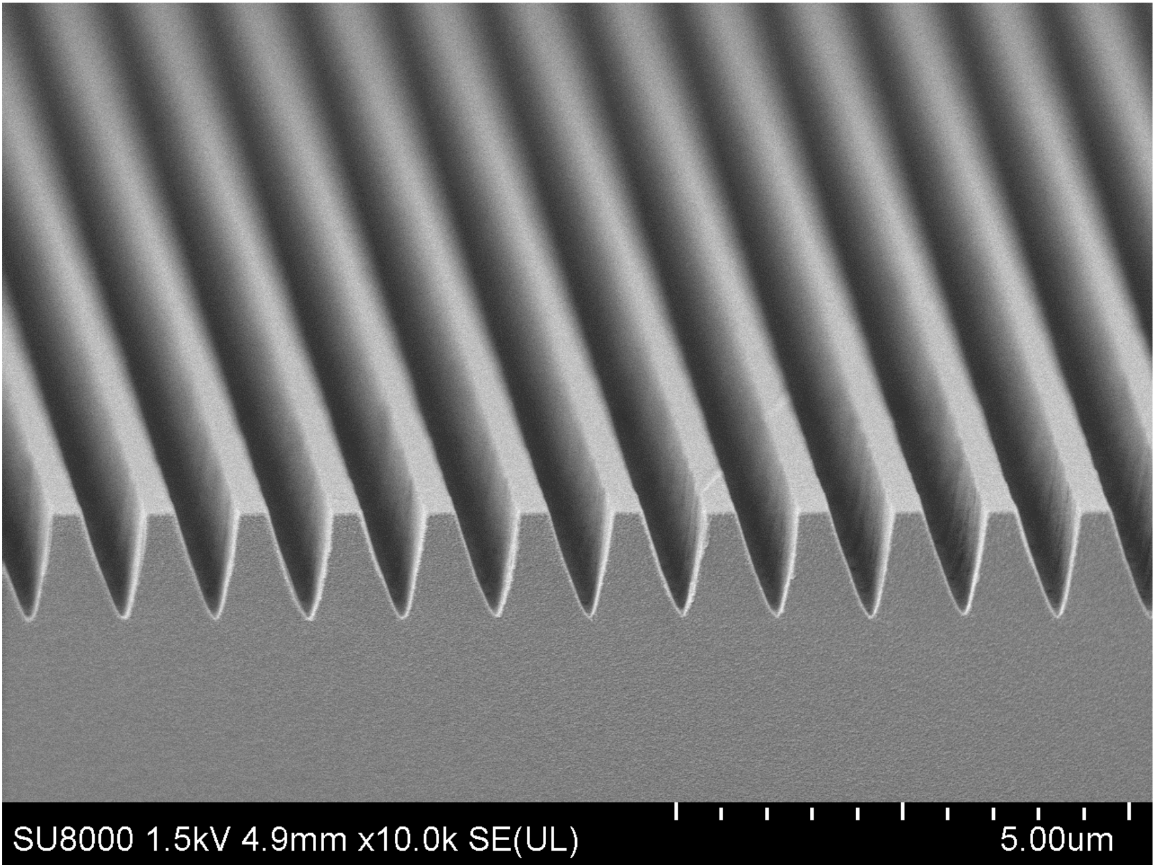
Optical metamaterials fabricated with nanoscale level structures have the ability to manipulate light in novel and more advantageous ways than possible with conventional optics. Optical metamaterials have opened up a plethora of practical applications including spectral selectivity, wavefront and polarization control, and the control of light radiation and detection. Current optical metasurface fabrication technologies utilize metasurface mask generation and pattern transfer processes that are not compatible with heat sensitive materials.
Heat sensitive materials such as piezoelectric and MEMS devices and assemblies, magnetic sensors, nonlinear optical crystals, laser glass or solid-state laser materials, etc. cannot be exposed to excess temperatures which in the context of this invention, means materials that cannot be exposed to temperatures greater than 50°C (122°F). LLNL’s invention describes a low-temperature method of fabricating bulk metamaterial structures based on a combination of compatible metasurface mask generation and pattern transfer processes.
Related LLNL technologies available for licensing
- Thin planar optical components generated with substrate-engraved metasurfaces
- Birefringent Waveplate and Method for Forming a Waveplate Having a Birefringent Metasurface
- Method of producing optical element with thicker substrate engraved metasurface layer
- Scalable Method of Forming Birefringent Optical Metasurfaces Operating at Very Short Wavelengths
- A Novel Method for Forming Waveplates from Common, Durable, Isotropic Optical Materials
- Enables optical metasurfaces to be fabricated on bulk materials not previously possible with current process methods.
- Creating optical metasurfaces on heat sensitive materials such as piezoelectric and MEMS devices and assemblies, magnetic sensors, nonlinear optical crystals, laser glass or solid-state laser materials, etc.
Current stage of technology development: TRL 3
LLNL has filed for patent protection on this invention.