
Optical phase plates, filters, holograms, Fresnel lenses and other diffractive optical elements are difficult to fabricate with arbitrarily tailored varying spatial structures, especially down to the micron scale and with high damage threshold. This method not only solves these challenges but further enables the possibility of fabricating many new optical elements that would not be possible otherwise from a greater variety of substrates materials (including sapphire) and operating over a great spectral range (including the UV).
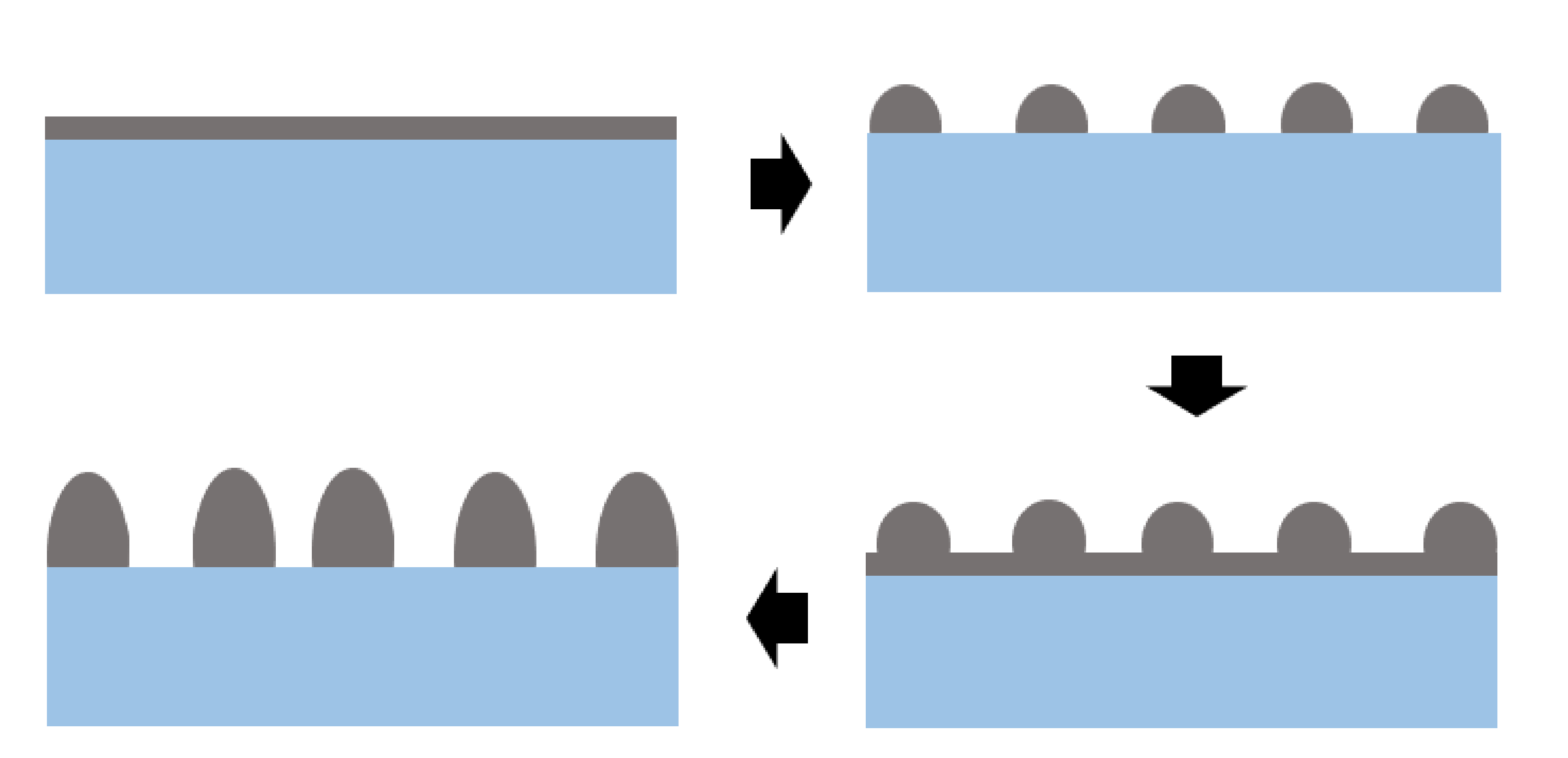
This invention (US Patent No. 11,294,103) is an extension of another LLNL invention, US Patent No. 10,612,145, which utilizes a thin sacrificial metal mask layer deposited on a dielectric substrate (e.g. fused silica) and subsequently nanostructured through a laser generated selective thermal de-wetting process. Local variation of the laser exposure controls the thermal de-wetting process yielding the mask’s desired metal nanoparticle distribution. The arbitrarily tailored sacrificial nanostructured mask is etched away through, for example, Reactive Ion Etching to leave the substrate with a subwavelength nanotextured surface that features an effective refractive index pattern imprinted from the mask structure. This specific invention (US Patent No. 11,294,103) achieves a thicker substrate-engraved meta-surface layer over US Patent No. 10,612,145 by using multiple depositions of the same or different metals layers to achieve the desired mask properties on different substrates with different dewetting characteristics and etch resistance.
Related LLNL technologies available for licensing
- Thin planar optical components generated with substrate-engraved metasurfaces
- Birefringent Waveplate and Method for Forming a Waveplate Having a Birefringent Metasurface
- Low-temperature fabrication method of bulk metamaterial structures for heat sensitive materials technology
- Scalable Method of Forming Birefringent Optical Metasurfaces Operating at Very Short Wavelengths
- A Novel Method for Forming Waveplates from Common, Durable, Isotropic Optical Materials
- Allows meta-surface engraving of a wider variety of substrates including sapphire.
- Allows deeper meta-surface engraving for broader spectral response including the UV.
- Allows for the arbitrary tailoring of the refractive index profile of a substrate surface layer down to the micron level.
- Featuring the high damage threshold of the intrinsic substrate material.
- Resulting refractive index pattern can be wavelength and angle insensitive (unlike thin film multi-layer dielectric solutions).
- Resulting surface texture is ultra-hydrophobic and is in principle self-cleaning.
- Produces arbitrarily large, but lightweight optical elements.
- Flexibility to pattern planar and non-planar surfaces.
- High power laser systems for industrial applications
- High energy lasers systems for scientific applications
Current stage of technology development: TRL 2-3
LLNL has patent(s) on this invention.
U.S. Patent No. 11,294,103 System and Method for Repeated Metal Deposition-Dewetting Steps to Form a Nano-Particle Etching Mask Producing Thicker Layer of Engraved Metasurface published 4/5/2022
U.S. Patent No. 10,612,145 Nanostructured layer for graded index freeform optics published 4/7/2020