
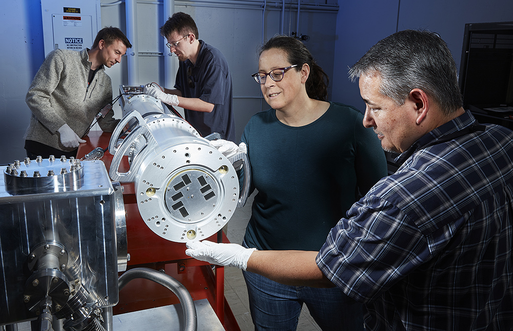
The Lawrence Livermore National Laboratory is home to the world’s largest laser system, the National Ignition Facility (NIF). The NIF with its 192 beam lines and over 40,000 optics has been an engine of innovation for lasers and optics technologies for the last couple of decades. The Lasers and Optics intellectual property portfolio is the culmination of the many groundbreaking developments in high energy, high peak power and ultrashort pulse laser system design and operation, including technologies related to Laser Diodes, Fiber & Disk Lasers, Compact Telescopes, High Damage Threshold Gratings, High Power Optical Components and their Fabrication and Coating Techniques. The thrust of the research and development at the NIF has been to realize novel approaches for laser systems, optical components and their applications that are more compact and higher efficiency while reliably delivering ever higher energy and peak power capabilities required in the furtherance of LLNL’s missions in Stockpile Stewardship and High Energy Density Science.
Portfolio News and Multimedia
The trade journal R&D World Magazine recently announced the winners of the awards, often called the “Oscars of innovation,” recognizing new commercial products, technologies and materials that are available for sale or license for their technological significance.
Lawrence Livermore National Laboratory (LLNL) scientists and engineers have earned four awards among the top 100 inventions worldwide. With this year’s results, the Laboratory has now collected a total of 186 R&D 100 awards since 1978.
Submitted through LLNL’s Innovation and Partnerships Office (IPO), these awards recognize the impact that Livermore innovation, in collaboration with industry partners, can have on the U.S. economy as well as globally.
Lawrence Livermore National Laboratory (LLNL) and Starris: Optimax Space Systems have signed a Cooperative Research and Development Agreement (CRADA), expanding production of LLNL’s next-generation space domain awareness technology. Starris will serve as the manufacturing partner that can scale production of monolithic telescope technology to meet the needs for proliferated constellations.
It’s the late 1990s. Lloyd Hackel and Brent Dane are researchers in Lawrence Livermore National Laboratory’s (LLNL) laser science and technology program.
They’re developing laser technology for X-ray lithography and satellite imaging research for the Department of Defense when the phone rings. On the line is Curtiss-Wright’s Metal Improvement Company (MIC) asking about something Hackel and Dane haven’t worked on before: high-peak-power laser peening for commercial applications in manufacturing.
This is an example of how LLNL’s mission-focused work advancing national security can lead to technology spin-offs with commercial importance through the Innovation and Partnerships Office (IPO).
For more, watch the YouTube video.

LLNL researchers developed a driver design for IFE-class lasers that allow for simultaneous high energy and high repetition rate operations. The LLNL invention integrates an amplifier head featuring a mosaic architecture with a modified high power diode delivery system that is designed to achieve uniform and geometry-match illumination of the mosaic structured amplifier module.

This invention works by imaging an ultrafast pulse diffracted from a large grating onto a spatial light modulator (SLM) thereby directly transcribing an arbitrary record on a pulse front tilted (PFT) ultrafast pulse. The grating generates PFT of the input pulse, and the SLM provides temporal control of the pulse through the space-to-time mapping of the tilted pulse. Coupling this patterned…
This invention exploits the non-linearities of optical Mach-Zehnder (MZ) electrooptic modulators to enhance small signal dynamic range at higher bandwidths. A linear photodiode (PD) converts the amplified optical signal output from the MZ back to an electrical signal completing an Electrical-Optical-Electrical (EOE) conversion cycle. The dynamic range can be further enhanced by daisy chaining…

This invention proposes to engineer the current density along the length of a laser diode to overcome the penalty associated with non-uniformity resulting from asymmetry in the gain, photon or carrier density despite having uniform contact. Optimizing the current density profile enables diode lasers to operate with greater power conversion efficiency or operate with equivalent power conversion…

This invention proposes to engineer the temperature dependence of the emission wavelength of LEDs and laser diodes. The approach is to use a strain-inducing coating to counteract the intrinsic temperature coefficient of the emission wavelength of the LED or laser diode device thereby rendering it athermal. This invention avoids additional complexity, size, weight and power dissipation of…

This invention proposes a method to overcome the key limitation of electrically pumped lasers based on AlN, AlGaN, or AlInGaN, namely the lack of suitable shallow donor and acceptor dopants. As the band gap of these materials increases (and the emission wavelength decreases), both electrons and holes require greater thermal energies in order to ionize.
Laser diode lensing effect can be substantially reduced by creating a pattern interface such that the substrate is only attached at the diode mesa. This is achieved by either creating a pattern solder joint and/or pattern substrate.
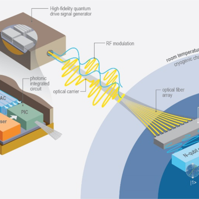
LLNL researchers in the NIF Directorate DoD Technologies RF Photonics Group explored phase modulation solutions to this signal processing challenge. Optical frequency combs offer phase noise characteristics that are orders of magnitude lower than available from commercial microwave references. The Photonics Group researchers recognized that by converting the intensity information into phase,…