
For this method, a Silicon on Insulator (SOI) wafer is used to tailor etch rates and thickness in initial steps of the process. The simple three step process approach is comprised of grayscale lithography, deep reactive-ion etch (DRIE) and liftoff of the SOI wafer. The liftoff process is used to dissolve the insulating layer, thus separating sections of the wafer as individual silicon…
Image
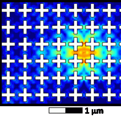
LLNL has developed a method of extending device lifetimes by imprinting into the device a shape that excludes specific vibrational modes, otherwise known as a phononic bandgap. Eliminating these modes prevents one of the primary energy loss pathways in these devices. LLNL’s new method enhances the coherence of superconducting circuits by introducing a phononic bandgap around the system’s…
Image

LLNL researchers have designed and tested performance characteristics for a multichannel pyrometer that works in the NIR from 1200 to 2000 nm. A single datapoint without averaging can be acquired in 14 microseconds (sampling rate of 70,000/s). In conjunction with a diamond anvil cell, the system still works down to about 830K.