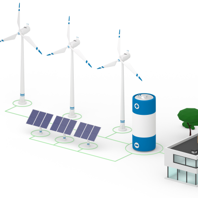
LLNL researchers have designed and produced, both conductive and non-conductive porous electrode components manufactured for improved metal deposition, discharging, and fluid dynamics in hybrid flow batteries. This is achieved through Direct Ink Writing (DIW) additive manufacturing. The engineered 3D electrodes enable uniform current distribution and even metal deposition during charging…
Image
The essence of this invention is a method that couples network architecture using neural implicit representations coupled with a novel parametric motion field to perform limited angle 4D-CT reconstruction of deforming scenes.
Image

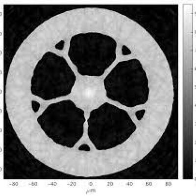
Improving the active material of the Zn anode is critical to improving the practicality of Zn-MnO2 battery technology. LLNL researchers have developed a new category of 3D structured Zn anode using a direct-ink writing (DIW) printing process to create innovative hierarchical architectures. The DIW ink, which is a gel-based mixture composed of zinc metal powder and organic binders, is extruded…
Image

For this method, a Silicon on Insulator (SOI) wafer is used to tailor etch rates and thickness in initial steps of the process. The simple three step process approach is comprised of grayscale lithography, deep reactive-ion etch (DRIE) and liftoff of the SOI wafer. The liftoff process is used to dissolve the insulating layer, thus separating sections of the wafer as individual silicon…
Image
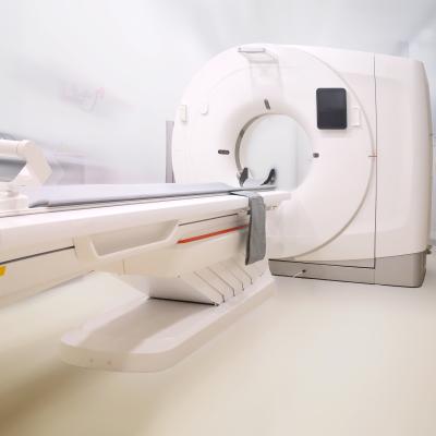
To solve these challenges using new and existing CT system designs, LLNL has developed an innovative software package for CT data processing and reconstruction. Livermore Tomography Tools (LTT) is a modern integrated software package that includes all aspects of CT modeling, simulation, reconstruction, and analysis algorithms based on the latest research in the field. LTT contains the most…
Image

LLNL researchers have designed and tested performance characteristics for a multichannel pyrometer that works in the NIR from 1200 to 2000 nm. A single datapoint without averaging can be acquired in 14 microseconds (sampling rate of 70,000/s). In conjunction with a diamond anvil cell, the system still works down to about 830K.
Image

LLNL has developed a compact and low-power cantilever-based sensor array, which has been used to detect various vapor-phase analytes. For further information on the latest developments, see the article "Sniffing the Air with an Electronic Nose."