The approach is to use appropriately doped semi-insulating gallium nitride to provide a high damage tolerant photoconductor with high responsivity to various pump wavelength light. Mn, C, or Fe are used as dopants to provide a source of electrons or holes that can be excited. This is combined with the use of dichroic antireflection coating at the GaN/polyimide/liquid crystal…
Keywords
- Show all (53)
- Imaging Systems (9)
- Photoconductive Semiconductor Switches (PCSS) (9)
- Semiconductors (7)
- Optical Switches (5)
- Power Electronics (4)
- Computing (2)
- Electric Grid (2)
- Sensors (2)
- Spectrometers (2)
- Analysis (1)
- Brain Computer Interface (BCI) (1)
- Compact Space Telescopes (1)
- Instrumentation (1)
- MEMS Sensors (1)
- Optical Sensors (1)
- Particle Accelerators (1)
- Quantum Science (1)
- (-) Additive Manufacturing (2)
- (-) 3D Electronics (1)
Image

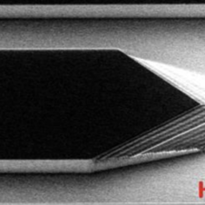
For this method, a Silicon on Insulator (SOI) wafer is used to tailor etch rates and thickness in initial steps of the process. The simple three step process approach is comprised of grayscale lithography, deep reactive-ion etch (DRIE) and liftoff of the SOI wafer. The liftoff process is used to dissolve the insulating layer, thus separating sections of the wafer as individual…
Image

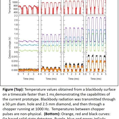
LLNL researchers have designed and tested performance characteristics for a multichannel pyrometer that works in the NIR from 1200 to 2000 nm. A single datapoint without averaging can be acquired in 14 microseconds (sampling rate of 70,000/s). In conjunction with a diamond anvil cell, the system still works down to about 830K.


