LLNL’s invention is a photopolymerizable polymer resin that consists of one or more nitrile-functional based polymers. The resin is formulated for SLA based 3D printing allowing for the production of nitrile-containing polymer components that can then be thermally processed into a conductive, highly graphitic materials. The novelty of the invention lies in (1) the photo-curable nitrile-…
Image

Image
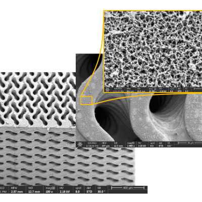
LLNL researchers have developed novel advanced manufactured biomimetic 3D-TPMS (triply periodic minimal surface) membrane architectures such as a 3D gyroid membrane. The membrane is printed using LLNL's nano-porous photoresist technology. LLNL’s 3D-TPMS membranes consist of two independent but interpenetrating macropore flow channel systems that are separated by a thin nano-porous wall. 3D-…
Image

For this method, a Silicon on Insulator (SOI) wafer is used to tailor etch rates and thickness in initial steps of the process. The simple three step process approach is comprised of grayscale lithography, deep reactive-ion etch (DRIE) and liftoff of the SOI wafer. The liftoff process is used to dissolve the insulating layer, thus separating sections of the wafer as individual silicon…
Image
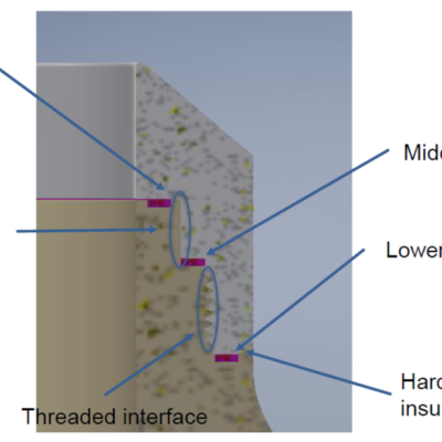
The approach is to build a high voltage insulator consisting of two materials: Poly-Ether-Ether-Ketone (“PEEK”) and Machinable Ceramic (“MACOR”). PEEK has a high stress tolerance but cannot withstand high temperatures, while MACOR has high heat tolerance but is difficult to machine and can be brittle. MACOR is used for the plasma-facing surface, while PEEK will handle the stresses and high…
Image
LLNL’s approach is to use their patented Photoconductive Charge Trapping Apparatus (U.S. Patent No. 11,366,401) as the active switch needed to discharge voltage across a vacuum gap in a particle accelerator, like the one described in their other patent (U.S. Patent No.
Image

LLNL has developed a compact and low-power cantilever-based sensor array, which has been used to detect various vapor-phase analytes. For further information on the latest developments, see the article "Sniffing the Air with an Electronic Nose."