
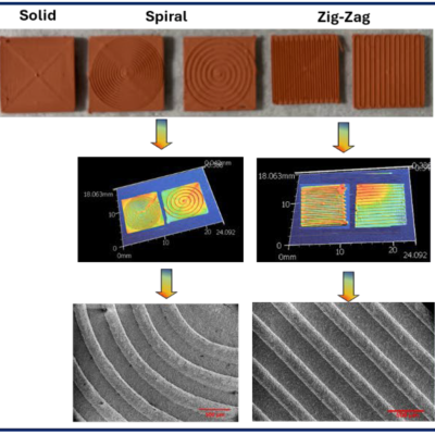
LLNL researchers has developed a composite copper current collector formulation readily used in DIW 3D printing to guide lithium-ion plating/dissolution during charging and discharging cycles.
Image

LLNL’s invention is a photopolymerizable polymer resin that consists of one or more nitrile-functional based polymers. The resin is formulated for SLA based 3D printing allowing for the production of nitrile-containing polymer components that can then be thermally processed into a conductive, highly graphitic materials. The novelty of the invention lies in (1) the photo-curable nitrile-…
Image
LLNL researchers have developed a fabrication process for creating 3D random interdigitated architectures of anodes and cathodes, eliminating the need for a membrane to separate them. This approach is similar to the repeating interdigitated multi-electrode architectures that also were developed at LLNL.
Image
LLNL researchers have developed novel advanced manufactured biomimetic 3D-TPMS (triply periodic minimal surface) membrane architectures such as a 3D gyroid membrane. The membrane is printed using LLNL's nano-porous photoresist technology. LLNL’s 3D-TPMS membranes consist of two independent but interpenetrating macropore flow channel systems that are separated by a thin nano-porous wall…
Image

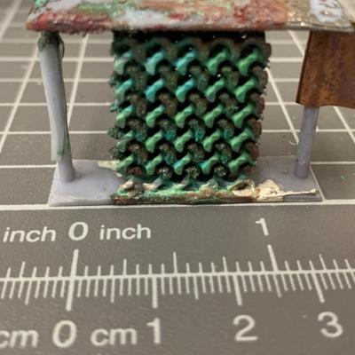
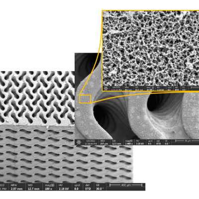
Improving the active material of the Zn anode is critical to improving the practicality of Zn-MnO2 battery technology. LLNL researchers have developed a new category of 3D structured Zn anode using a direct-ink writing (DIW) printing process to create innovative hierarchical architectures. The DIW ink, which is a gel-based mixture composed of zinc metal powder and organic binders, is…
Image
To get the best of both worlds – the sensitivity of LC-MS with the speed of PS-MS – and a functional substrate that can maintain sample integrity, LLNL researchers looked to 3D printing. They have patented a novel approach to create lattice spray substrates for direct ionization mass spectroscopy using 3D-printing processes.
Image

For this method, a Silicon on Insulator (SOI) wafer is used to tailor etch rates and thickness in initial steps of the process. The simple three step process approach is comprised of grayscale lithography, deep reactive-ion etch (DRIE) and liftoff of the SOI wafer. The liftoff process is used to dissolve the insulating layer, thus separating sections of the wafer as individual…
Image

LLNL researchers, through careful control over the chemistry, network formation, and crosslink density of the ink formulations as well as introduction of selected additives, have been successful in preparing 3D printable silicone inks with tunable material properties. For DIW (direct in writing) applications, LLNL has a growing IP portfolio around 3D printable silicone feedstocks for…
LLNL’s method of 3D printing fiber-reinforced composites has two enabling features:
Image

LLNL’s Optically-based Interstory Drift Meter System provides a means to accurately measure the dynamic interstory drift of a vibrating building (or other structure) during earthquake shaking. This technology addresses many of the shortcomings associated with traditional strong motion accelerometer based building monitoring.
LLNL’s discrete diode position sensitive device is a newly…