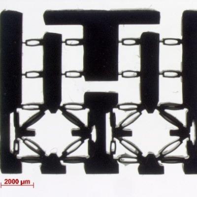
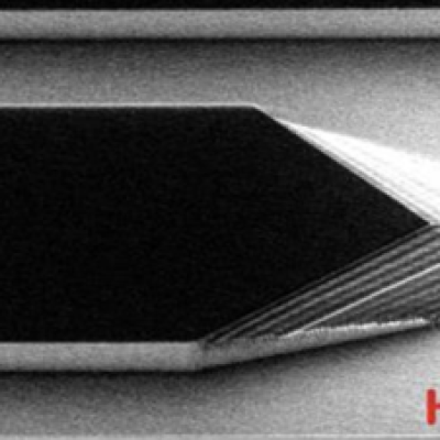
For this method, a Silicon on Insulator (SOI) wafer is used to tailor etch rates and thickness in initial steps of the process. The simple three step process approach is comprised of grayscale lithography, deep reactive-ion etch (DRIE) and liftoff of the SOI wafer. The liftoff process is used to dissolve the insulating layer, thus separating sections of the wafer as individual silicon…
Keywords
- Show all (50)
- Photoconductive Semiconductor Switches (PCSS) (9)
- Imaging Systems (8)
- Semiconductors (6)
- Optical Switches (4)
- Power Electronics (3)
- Sensors (3)
- Computing (2)
- Electric Grid (2)
- MEMS Sensors (2)
- Optical Sensors (2)
- Particle Accelerators (2)
- Spectrometers (2)
- Additive Manufacturing (1)
- Quantum Science (1)
- Simulation (1)
- (-) 3D Electronics (1)
- (-) Precision Engineering (1)

Recent advancements in additive manufacturing, also called 3D printing, allow precise placement of materials in three dimensions. LLNL researchers have invented mechanical logic gates based on flexures that can be integrated into the microstructure of a micro-architected material through 3D printing. The logic gates can be combined into circuits allowing complex logic operations to be…

The technology that is available has the capability to inject realistic radiation detection spectra into the amplifier of a radiation detector and produce the all the observables that are available with that radiation detection instrument; count-rate, spectrum, dose rate, etc.
The system uses the capability of LLNL to generate the source output for virtually any source and determine…

