
A thyristor will stay conducting until the current through the device is zero (“current zero”) or perhaps slightly negative. LLNL’s approach is to use the opticondistor (“OTV”) to force this current zero in order to force the device into an “off” state. By combining a light-activated thyristor with an OTV, a noise-immune, high efficiency, high-power switching device can be constructed. The…
Image

The researchers’ approach leverages the concept that dopants have high diffusivities in Ga2O3; the key lies in the selection of the appropriate dopant. This LLNL invention describes two device types that employ this design:
Image

This invention proposes to engineer the current density along the length of a laser diode to overcome the penalty associated with non-uniformity resulting from asymmetry in the gain, photon or carrier density despite having uniform contact. Optimizing the current density profile enables diode lasers to operate with greater power conversion efficiency or operate with equivalent power conversion…
Image

This invention proposes to engineer the temperature dependence of the emission wavelength of LEDs and laser diodes. The approach is to use a strain-inducing coating to counteract the intrinsic temperature coefficient of the emission wavelength of the LED or laser diode device thereby rendering it athermal. This invention avoids additional complexity, size, weight and power dissipation of…
Image

This invention proposes a method to overcome the key limitation of electrically pumped lasers based on AlN, AlGaN, or AlInGaN, namely the lack of suitable shallow donor and acceptor dopants. As the band gap of these materials increases (and the emission wavelength decreases), both electrons and holes require greater thermal energies in order to ionize.
Image
Laser diode lensing effect can be substantially reduced by creating a pattern interface such that the substrate is only attached at the diode mesa. This is achieved by either creating a pattern solder joint and/or pattern substrate.
Image

Design and construction of a photoconductive switch requires a diamond photoconductor illuminated by light of a certain excitation wavelength.
Characteristics of the LLNL-developed switch are as follows:
Image
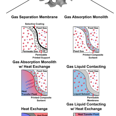
Hierarchical Triply Periodic Minimal Surface Structures For Efficient Two Fluid Flow Reactor Designs
LLNL researchers have devised a set of design principles that facilitates the development of practical TPMS-based two fluid flow reactors.; included in the design are these new concepts:
Image

LLNL researchers have invented an ultrafast PCSS to drive a high-power laser diode with arbitrary pulse widths. These devices operate by supplying a high voltage (>10 kV) to one side of the switch. A short pulse of light illuminates the semiconductor, instantly turning it from highly resistive to highly conductive.
Image
![Filled (8,8) (left) and (15,15) (right) CNTs with [EMIM+][BF4- ] using SGTI with the proposed spliced soft-core potential (SSCP) approach](/sites/default/files/styles/scale_exact_400x400_/public/2023-10/Filled%20CNTs%20using%20SGTI.png?itok=Dy0ObN7i)
LLNL researchers have developed a novel simulation methodology using slow growth thermodynamic integration (SGTI) utilizing spliced soft-core interaction potential (SSCP). The approach to filling the molecular enclosures is a nonphysical one. Rather than filling the pores from the open ends this method creates steps in the algorithm that allow molecules to pass through the pore wall and…
Image

U.S. Patent No. 11,555,965 describes LLNL’s invention of “Illumination Frustums” for photoconductive switches to capture and “frustrate” the light from leaving the frustum. LLNL researcher’s latest novel invention, “Twister Oven”, achieves this by encouraging laser light absorption in a photo conductor material. Light enters the oven twisting and reflecting, making near normal incident multi…
Image
Design and construction of a photoconductive switch requires a diamond photoconductor illuminated by light of a certain excitation wavelength. The diamond material is chosen to be doped with substitutional nitrogen to act as a source of electrons. The device architecture allows maximum light entering the aperture. The top and bottom electrodes are made of ultra-wide bandgap (UWBG)…
Image

LLNL researchers faced this challenge by bridging the gap between VEDs and solid-state electronics (SSE). Their approach was to create a hybrid vacuum microelectronic device (VMD) architecture that combines the properties of vacuum as the electronic medium and the compact form factor and manufacturing scalability of semiconductor microelectronic chips.
Image

Design and construction of a photoconductive switch requires a diamond photoconductor illuminated by light of a certain excitation wavelength. The diamond material is specifically doped with substitutional nitrogen, which act as a source of electrons. The device architecture allows maximum light entering the aperture. The top and bottom electrodes are made of ultra wide band gap (UWBG)…
Image

The approach is to use a custom-designed frustrum and attach it to the optical fiber that connects to the PCSS. Light from the fiber enters the frustrum, spreads out, and enters the PCSS. Any unabsorbed light re-enters the frustrum and, because of its geometry, reflects back into the PCSS itself with only a negligible fraction escaping from the fiber. The shape of the novel frustrum is…
Image

Recent advancements in additive manufacturing, also called 3D printing, allow precise placement of materials in three dimensions. LLNL researchers have invented mechanical logic gates based on flexures that can be integrated into the microstructure of a micro-architected material through 3D printing. The logic gates can be combined into circuits allowing complex logic operations to be…
Image
The LLNL method for optimizing as built optical designs uses insights from perturbed optical system theory and reformulates perturbation of optical performance in terms of double Zernikes, which can be calculated analytically rather than by tracing thousands of rays. A new theory of compensation is enabled by the use of double Zernikes which allows the performance degradation of a perturbed…
Image

By combining 3D printing and dealloying., researchers at LLNL have developed a method for fabricating metal foams with engineered hierarchical architectures consisting of pores at least 3 distinct length scales. LLNL’s method uses direct ink writing (DIW), a 3D printing technique for additive manufacturing to fabricate hierarchical nanoporous metal foams with deterministically controlled 3D…
Image

To overcome limitations with cellular silicone foams, LLNL innovators have developed a new 3D energy absorbing material with tailored/engineered bulk-scale properties. The energy absorbing material has 3D patterned architectures specially designed for specific energy absorbing properties. The combination of LLNL's capabilities in advanced modeling and simulation and the additive…