LLNL researchers have developed a TDLAS-based, standalone, real-time gas analyzer in a small form-factor for continuous or single-point monitoring. The system can analyze multiple gases with ultra-high sensitivity (ppm detection levels) in harsh conditions when utilizing wavelength-modulation spectroscopy (WMS).
Image

For this method, a Silicon on Insulator (SOI) wafer is used to tailor etch rates and thickness in initial steps of the process. The simple three step process approach is comprised of grayscale lithography, deep reactive-ion etch (DRIE) and liftoff of the SOI wafer. The liftoff process is used to dissolve the insulating layer, thus separating sections of the wafer as individual silicon…
Image
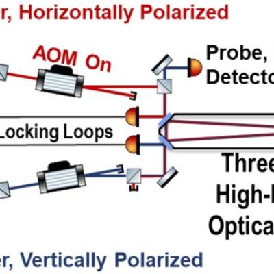
LLNL’s novel approach combines 2-color spectroscopy with CRDS, a combination not previously utilized.
Image

Recent advancements in additive manufacturing, also called 3D printing, allow precise placement of materials in three dimensions. LLNL researchers have invented mechanical logic gates based on flexures that can be integrated into the microstructure of a micro-architected material through 3D printing. The logic gates can be combined into circuits allowing complex logic operations to be…