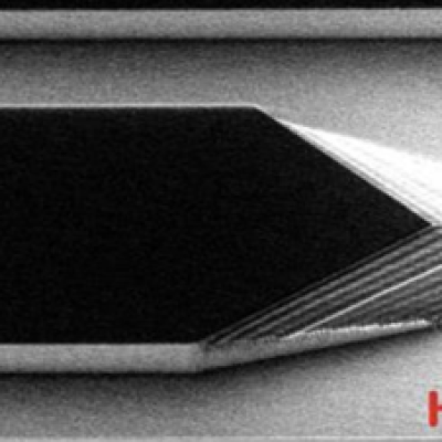
For this method, a Silicon on Insulator (SOI) wafer is used to tailor etch rates and thickness in initial steps of the process. The simple three step process approach is comprised of grayscale lithography, deep reactive-ion etch (DRIE) and liftoff of the SOI wafer. The liftoff process is used to dissolve the insulating layer, thus separating sections of the wafer as individual silicon…
Keywords
- Show all (101)
- Additive Manufacturing (37)
- Photoconductive Semiconductor Switches (PCSS) (9)
- Imaging Systems (8)
- 3D Printing (7)
- Semiconductors (6)
- Optical Switches (4)
- Electric Grid (3)
- Manufacturing Improvements (3)
- Power Electronics (3)
- Sensors (3)
- Computing (2)
- Optical Sensors (2)
- Particle Accelerators (2)
- Precision Engineering (2)
- Spectrometers (2)
- Synthesis and Processing (2)
- Manufacturing Simulation (1)
- Volumetric Additive Manufacturing (1)
- (-) Manufacturing Automation (2)
- (-) MEMS Sensors (2)
Technology Portfolios
Image

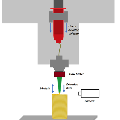
Livermore researchers have developed a method for implementing closed-loop control in extrusion printing processes by means of novel sensing, machine learning, and optimal control algorithms for the optimization of printing parameters and controllability. The system includes a suite of sensors, including cameras, voltage and current meters, scales, etc., that provide in-situ process monitoring…
Image

LLNL researchers have developed a system that relies on machine learning to monitor microfluidic devices. The system includes (at least) a microfluidic device, sensor(s), and a local network computer. The system could also include a camera that takes real-time images of channel(s) within an operating microfluidic device. A subset of these images can be used to train/teach a machine learning…
Image

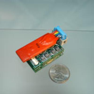
LLNL has developed a compact and low-power cantilever-based sensor array, which has been used to detect various vapor-phase analytes. For further information on the latest developments, see the article "Sniffing the Air with an Electronic Nose."

