
For this method, a Silicon on Insulator (SOI) wafer is used to tailor etch rates and thickness in initial steps of the process. The simple three step process approach is comprised of grayscale lithography, deep reactive-ion etch (DRIE) and liftoff of the SOI wafer. The liftoff process is used to dissolve the insulating layer, thus separating sections of the wafer as individual silicon…
Image
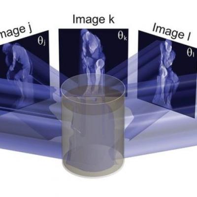
LLNL has developed a system and method that accomplishes volumetric fabrication by applying computed tomography (CT) techniques in reverse, fabricating structures by exposing a photopolymer resin volume from multiple angles, updating the light field at each angle. The necessary light fields are spatially and/or temporally multiplexed, such that their summed energy dose in a target resin volume…
Image

LLNL has developed a compact and low-power cantilever-based sensor array, which has been used to detect various vapor-phase analytes. For further information on the latest developments, see the article "Sniffing the Air with an Electronic Nose."