
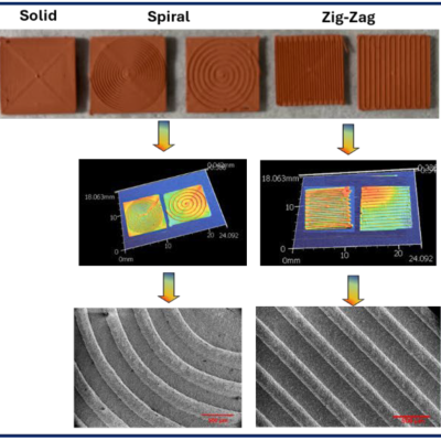
LLNL researchers has developed a composite copper current collector formulation readily used in DIW 3D printing to guide lithium-ion plating/dissolution during charging and discharging cycles.
Image
This invention focuses on the design of a fully interchangeable hub-droplet device apparatus for multiple droplet generation in parallel. The novel central hub combined with interchangeable chip configuration allows the use of different planar droplet generation devices that can be replaced and exchanged as needed. By separating the central housing hub which distributes incoming liquids into…
Image

For this method, a Silicon on Insulator (SOI) wafer is used to tailor etch rates and thickness in initial steps of the process. The simple three step process approach is comprised of grayscale lithography, deep reactive-ion etch (DRIE) and liftoff of the SOI wafer. The liftoff process is used to dissolve the insulating layer, thus separating sections of the wafer as individual…
Image

Livermore researchers have developed a method of fabricating functional polymer-based particles by crosslinking UV-curable polymer drops in mid-air and collecting crosslinked particles in a solid container, a liquid suspension, or an air flow. Particles could contain different phases in the form or layered structures that contain one to multiple cores, or structures that are blended with…