Image
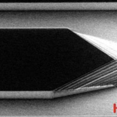
SEM image of a prototype for a neural implant shuttle etched into a non-SOI wafer. The 7:1 (Si:Photoresist) etch selectivity used here allowed for a maximum structure height of 32 μm, with up to 75 steps of 0.4 μm height each. Scale bar 100 μm.

For this method, a Silicon on Insulator (SOI) wafer is used to tailor etch rates and thickness in initial steps of the process.  The simple three step process approach is comprised of grayscale lithography, deep reactive-ion etch (DRIE) and liftoff of the SOI wafer.  The liftoff process is used to dissolve the insulating layer, thus separating sections of the wafer as individual silicon…

Image
AgAg2S reference electrode

LLNL has developed a reference electrode that is a great improvement on the widely used silver or platinum wire QRE commonly used in electrochemistry in ionic liquids. This new reference electrode, based on a silver-sulfide coated silver wire, exhibits greatly improved stability over a QRE. The stability of our RE approaches that of the Ag/Ag+ RE, but unlike the Ag/Ag+ RE, the RE reported here…