
A thyristor will stay conducting until the current through the device is zero (“current zero”) or perhaps slightly negative. LLNL’s approach is to use the opticondistor (“OTV”) to force this current zero in order to force the device into an “off” state. By combining a light-activated thyristor with an OTV, a noise-immune, high efficiency, high-power switching device can be constructed. The…
Image

The researchers’ approach leverages the concept that dopants have high diffusivities in Ga2O3; the key lies in the selection of the appropriate dopant. This LLNL invention describes two device types that employ this design:
Image

This invention proposes to engineer the current density along the length of a laser diode to overcome the penalty associated with non-uniformity resulting from asymmetry in the gain, photon or carrier density despite having uniform contact. Optimizing the current density profile enables diode lasers to operate with greater power conversion efficiency or operate with equivalent power conversion…
Image

This invention proposes to engineer the temperature dependence of the emission wavelength of LEDs and laser diodes. The approach is to use a strain-inducing coating to counteract the intrinsic temperature coefficient of the emission wavelength of the LED or laser diode device thereby rendering it athermal. This invention avoids additional complexity, size, weight and power dissipation of…
Image

This invention proposes a method to overcome the key limitation of electrically pumped lasers based on AlN, AlGaN, or AlInGaN, namely the lack of suitable shallow donor and acceptor dopants. As the band gap of these materials increases (and the emission wavelength decreases), both electrons and holes require greater thermal energies in order to ionize.
Image
Laser diode lensing effect can be substantially reduced by creating a pattern interface such that the substrate is only attached at the diode mesa. This is achieved by either creating a pattern solder joint and/or pattern substrate.
Image

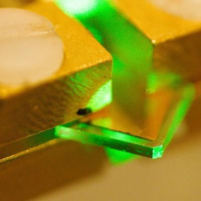
Design and construction of a photoconductive switch requires a diamond photoconductor illuminated by light of a certain excitation wavelength.
Characteristics of the LLNL-developed switch are as follows:
Image

LLNL researchers has developed designs to augment WBG/UWBG-based OALVs to improve their power handling capability under CW operational environments. These designs include:
Image

LLNL researchers have invented an ultrafast PCSS to drive a high-power laser diode with arbitrary pulse widths. These devices operate by supplying a high voltage (>10 kV) to one side of the switch. A short pulse of light illuminates the semiconductor, instantly turning it from highly resistive to highly conductive.
Image

U.S. Patent No. 11,555,965 describes LLNL’s invention of “Illumination Frustums” for photoconductive switches to capture and “frustrate” the light from leaving the frustum. LLNL researcher’s latest novel invention, “Twister Oven”, achieves this by encouraging laser light absorption in a photo conductor material. Light enters the oven twisting and reflecting, making near normal incident multi…
Image
Design and construction of a photoconductive switch requires a diamond photoconductor illuminated by light of a certain excitation wavelength. The diamond material is chosen to be doped with substitutional nitrogen to act as a source of electrons. The device architecture allows maximum light entering the aperture. The top and bottom electrodes are made of ultra-wide bandgap (UWBG)…
Image

LLNL researchers faced this challenge by bridging the gap between VEDs and solid-state electronics (SSE). Their approach was to create a hybrid vacuum microelectronic device (VMD) architecture that combines the properties of vacuum as the electronic medium and the compact form factor and manufacturing scalability of semiconductor microelectronic chips.
Image

Design and construction of a photoconductive switch requires a diamond photoconductor illuminated by light of a certain excitation wavelength. The diamond material is specifically doped with substitutional nitrogen, which act as a source of electrons. The device architecture allows maximum light entering the aperture. The top and bottom electrodes are made of ultra wide band gap (UWBG)…
Image

The approach is to use a custom-designed frustrum and attach it to the optical fiber that connects to the PCSS. Light from the fiber enters the frustrum, spreads out, and enters the PCSS. Any unabsorbed light re-enters the frustrum and, because of its geometry, reflects back into the PCSS itself with only a negligible fraction escaping from the fiber. The shape of the novel frustrum is…
Image

LLNL’s Optically-based Interstory Drift Meter System provides a means to accurately measure the dynamic interstory drift of a vibrating building (or other structure) during earthquake shaking. This technology addresses many of the shortcomings associated with traditional strong motion accelerometer based building monitoring.
LLNL’s discrete diode position sensitive device is a newly…
Image

The Optical Transconductance Varistor (OTV, formerly Opticondistor) overcomes depletion region voltage limitations by optically exciting wide bandgap materials in a compact package. A 100μm thick crystal could have the capability approaching 40kV and would replace numerous equivalent junction devices. Thus, unlike present junction transistors or diodes, this wide bandgap device can be stacked…
Image

The invention relates to a measurement method and system for capturing both the amplitude and phase temporal profile of a transient waveform or a selected number of consecutive waveforms having bandwidths of up to about 10 THz in a single shot or in a high repetition rate mode. The invention consists of an optical preprocessor which can then output a time-scaled replica of the input signal to…