

For this method, a Silicon on Insulator (SOI) wafer is used to tailor etch rates and thickness in initial steps of the process. The simple three step process approach is comprised of grayscale lithography, deep reactive-ion etch (DRIE) and liftoff of the SOI wafer. The liftoff process is used to dissolve the insulating layer, thus separating sections of the wafer as individual…
Image
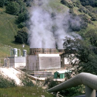
LLNL has a patented process to produce colloidal silica directly from geothermal fluids. Livermore’s process uses membranes to produce a mono-dispense slurry of colloidal silica particles for which there are several applications. LLNL has demonstrated that colloidal silica solutions that result from extraction of silica from geothermal fluids undergo a transition to a solid gel over a range of…