
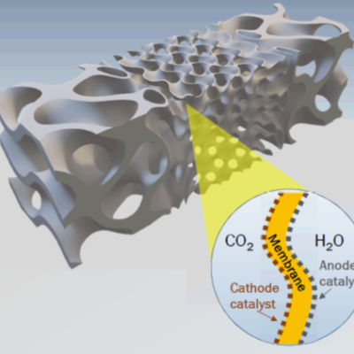
LLNL inventors have developed a gas diffusion electrode (GDE) architecture employing a multi-stack design. The first layer consists of a physical vapor deposited metallic catalyst film which then has a second composite layer deposited on top consisting of a second catalyst material mixed with a polymer electrolytes. The two layers working in tandem allow for near 100% CO…
Image
The approach is to use foundational materials science, structural design, thermal analysis, optic fabrication, and space systems engineering, and to use optimize them through large-scale simulation to realize meter-scale telescopes at 10X cost reduction. LLNL’s folded Gregorian design integrates all alignment sensitive components into one static monolithic system. Like solid-…
Image

The approach is to use appropriately doped semi-insulating gallium nitride to provide a high damage tolerant photoconductor with high responsivity to various pump wavelength light. Mn, C, or Fe are used as dopants to provide a source of electrons or holes that can be excited. This is combined with the use of dichroic antireflection coating at the GaN/polyimide/liquid crystal…
Image
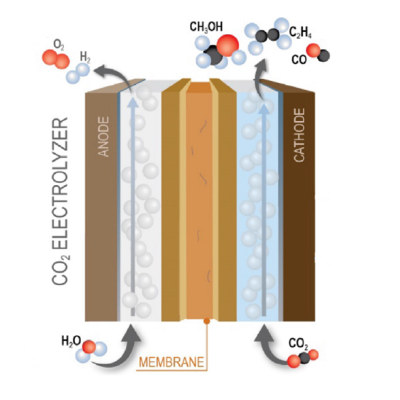
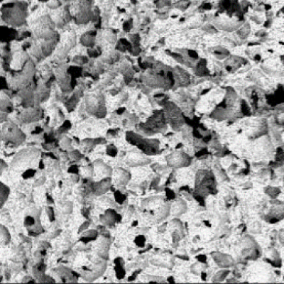
LLNL’s researchers use physical vapor deposition (sputter deposition or electron beam deposition) to coat an inert gasket material (i.e. PTFE) with a conductive metal (i.e. copper). The gas diffusion electrode overlaps onto the copper coated gasket to allow for electrical conductivity between the catalyst surface and the flow field/current collector of a CO2 electrolyzer. The coated gasket…
Image
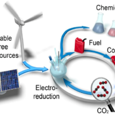
Using their computational design optimization, LLNL researchers have developed copper-based dilute alloy catalysts (contains <10 at.% of the minority metal alloy component) and demonstrated these novel catalysts have improved energy efficiency and selectivity of the methane conversion reaction. By alloying copper with a small amount of the electropositive minority metal element, the…
Image
Rapid monolith development at scale is achieved through use of a functionally equivalent optic simulant made from a low-cost material to substitute the functional optic. Monolith optical performance is affected not only by thermal expansion but also by temperature inhomogeneity due to the temperature dependence of refractive index.
Image
Aeroptics are a proposed new class of monolithic optical system in aerogel fabricated by molding around a master mandrel. This approach combines the intrinsic stability of proven monolithic telescopes, with the ultralow density of silica aerogels. In Aeroptics, the monolith is hollow with an aerogel substrate providing a supporting structure. Theoretically, Aeroptics could enable 1-m aperture…
Image

LLNL researchers has developed designs to augment WBG/UWBG-based OALVs to improve their power handling capability under CW operational environments. These designs include:
Image
This invention achieves both a wider field of view and faster f-number within a monolithic substrate by incorporating an aspheric convex refractive first surface and a planar aspheric field corrector surface on the final refractive surface. These two refractive surfaces work in conjunction with a concave aspheric primary and convex aspheric secondary mirror (e.g. Cassegrain type) to improve…
Image
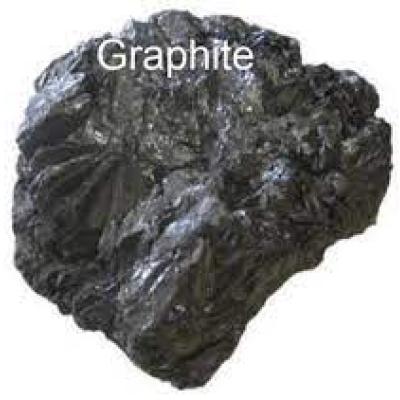
LLNL’s innovation offers an alternate synthetic route to graphite at lower cost using a molten salt mixture of CaCl2-CaCO3-CaO. The synthetic production of graphite and other high-value carbon materials is accomplished in molten salt media via electrochemical reduction and transformation of the carbon from the carbonate ion. The broad electrochemical window of molten salts enables the…
Image

Design and construction of a photoconductive switch requires a diamond photoconductor illuminated by light of a certain excitation wavelength. The diamond material is specifically doped with substitutional nitrogen, which act as a source of electrons. The device architecture allows maximum light entering the aperture. The top and bottom electrodes are made of ultra wide band…
Image

The approach is to use a custom-designed frustrum and attach it to the optical fiber that connects to the PCSS. Light from the fiber enters the frustrum, spreads out, and enters the PCSS. Any unabsorbed light re-enters the frustrum and, because of its geometry, reflects back into the PCSS itself with only a negligible fraction escaping from the fiber. The shape of the novel…
Image
The novel LLNL approach is to use projection microstereolithography (LAPµSL), starting with a photocurable methacrylate resin formulation consisting of a combination of a photoinitiator, photoabsorber, inhibitor, solvents, and other additives. Prior to use, the resin is pretreated to control viscosity for easier handling. The resin is fed to a LAPµSL printer which employs a near UV…
Image
The inventors have developed a 3% Yttria partially-stabilized Zirconia (3YZ) ceramic ink that produces parts with both nano and microporosity and is compatible with two AM techniques: DIW and projection microstereolithography (PμSL). The 3YZ nano-porous ceramic printed parts had engineered macro cavities measuring several millimeters in length, wall thicknesses ranging from 200 to 540 μm, and…
Image
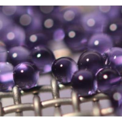
This invention describes a multiple nozzle microfluidic unit that allows simultaneous generation streams of multiple layered coaxial liquid jets. Liquids are pumped into the device at a combined flow rate from 100 mL/hr to 10 L/hr. Droplets are created with diameters in the range of 1 µm to 5 mm and can be created with 1-2 shell layers encapsulating fluid. Droplets created from the system can…
Image

Monolithic Telescopes are a novel implementation of a solid catadioptric design form, instantiated in a monolithic block of fused silica.
Image
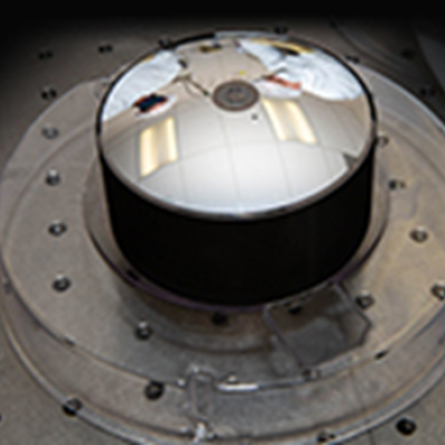
LLNL is developing the Space-based Telescopes for Actionable Refinement of Ephemeris (STARE). STARE is a constellation of low cost nano-satellites (less than 5Kg) in low-earth orbit dedicated to the observation of space debris in conjunction with a ground-based infrastructure for maintenance, coordination and data processing. Each nano-satellite in the constellation is capable of recording an…
Image

The Optical Transconductance Varistor (OTV, formerly Opticondistor) overcomes depletion region voltage limitations by optically exciting wide bandgap materials in a compact package. A 100μm thick crystal could have the capability approaching 40kV and would replace numerous equivalent junction devices. Thus, unlike present junction transistors or diodes, this wide bandgap device can be stacked…