

The approach is to use appropriately doped semi-insulating gallium nitride to provide a high damage tolerant photoconductor with high responsivity to various pump wavelength light. Mn, C, or Fe are used as dopants to provide a source of electrons or holes that can be excited. This is combined with the use of dichroic antireflection coating at the GaN/polyimide/liquid crystal…
Image

Powder atomic layer deposition process is used to coat nanopowders of host materials (e.g. yttrium aluminum garnet) with optically active neodymium organometal precursor followed by O2/O3 RF plasma to convert to a single layer of Nd2O3. The process can be repeated to build arbitrarily thick layers with custom doping profiles and followed by post-…
Image

A thyristor will stay conducting until the current through the device is zero (“current zero”) or perhaps slightly negative. LLNL’s approach is to use the opticondistor (“OTV”) to force this current zero in order to force the device into an “off” state. By combining a light-activated thyristor with an OTV, a noise-immune, high efficiency, high-power switching device can be…
Image

This invention proposes using a pulse laser configured to generate laser pulses and a controller for controlling operation of the pulse laser. The controller is further configured to control the pulse laser to cause the pulse laser to generate at least one of the laser pulses with a spatiotemporally varying laser fluence over a duration of at least one of the laser pulses. The spatiotemporally…
Image

LLNL researchers has developed designs to augment WBG/UWBG-based OALVs to improve their power handling capability under CW operational environments. These designs include:
Image

The approach is to leverage the fact that a momentary “load” equal to the power transmission line impedance, (Z0), during the transient can suppress its propagation. Z(0) is typically a fixed impedance of several hundred ohms based on the geometry of most single wire transmission lines.
So, an isolated self-powered opticondistor (OTV) system may provide an ultrafast method of…
Image

LLNL’s novel approach to enable MVDC power systems to operate safely is to develop a wideband gap bulk optical semiconductor switch (WBG BOSS) circuit breaker. For higher power, efficiency and temperature operation, vanadium-doped silicon carbide (V-doped SiC) appears to be the most promising basis for WBG BOSS circuit breaker (other dopants like aluminum, boron and nitrogen may further…
Image
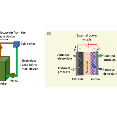
LLNL researchers has developed an approach to mitigate HER on the ‘plating’ electrode, which uses a sub-device as a rebalancing cell to restore electrolyte properties, including pH, conductivity, and capacity across the main device of the flow battery. This sub-device, which may need to be powered externally, has three major physical components: (1) a cathode electrode, (2) an anode…
Image

LLNL has developed a novel methodology for using commercially available automated sensors and actuators which can be deployed at scale in large appliances and plug-in EVs to provide as needed electric grid stabilization capabilities. The approach comprises of a population of voltage relays with a range of setpoints that would gradually reduce load as voltage falls. More severe voltage…
Image

Improving the active material of the Zn anode is critical to improving the practicality of Zn-MnO2 battery technology. LLNL researchers have developed a new category of 3D structured Zn anode using a direct-ink writing (DIW) printing process to create innovative hierarchical architectures. The DIW ink, which is a gel-based mixture composed of zinc metal powder and organic binders, is…
Image
To address many of the aforementioned challenges of manufacturing LIBs and SSBs, LLNL researchers have developed a number of inventions that offer proposed solutions for their components:
Image

Design and construction of a photoconductive switch requires a diamond photoconductor illuminated by light of a certain excitation wavelength. The diamond material is specifically doped with substitutional nitrogen, which act as a source of electrons. The device architecture allows maximum light entering the aperture. The top and bottom electrodes are made of ultra wide band…
Image

The approach is to use a custom-designed frustrum and attach it to the optical fiber that connects to the PCSS. Light from the fiber enters the frustrum, spreads out, and enters the PCSS. Any unabsorbed light re-enters the frustrum and, because of its geometry, reflects back into the PCSS itself with only a negligible fraction escaping from the fiber. The shape of the novel…
Image

Livermore Lab researchers have developed two new methods for improving the efficiency of laser drilling. The first method is based on multi-pulse laser technology. Two synchronized free-running laser pulses from a tandem-head Nd:YAG laser and a gated CW laser are capable of drilling through 1/8-in-thick stainless-steel targets at a standoff distance of 1 m without gas-assist. The combination of a…
Image

The new LLNL technique works by transiently removing and trapping concrete or rock surface material, so that contaminants are confined in a manner that is easy to isolate and remove. Our studies suggest that 10 m2 of surface could be processed per hour. The technique easily scales to more surface/hr.
Image

The Optical Transconductance Varistor (OTV, formerly Opticondistor) overcomes depletion region voltage limitations by optically exciting wide bandgap materials in a compact package. A 100μm thick crystal could have the capability approaching 40kV and would replace numerous equivalent junction devices. Thus, unlike present junction transistors or diodes, this wide bandgap device can be stacked…