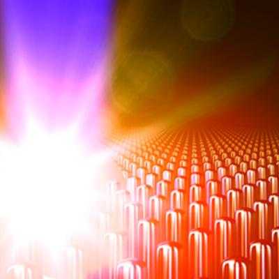
The approach is to use appropriately doped semi-insulating gallium nitride to provide a high damage tolerant photoconductor with high responsivity to various pump wavelength light. Mn, C, or Fe are used as dopants to provide a source of electrons or holes that can be excited. This is combined with the use of dichroic antireflection coating at the GaN/polyimide/liquid crystal…
Keywords
- Show all (44)
- Substrate Engraved Meta-Surface (SEMS) (7)
- Compact Space Telescopes (6)
- Diode Lasers (5)
- Precision Optical Finishing (4)
- Optical Damage Mitigation (3)
- RF Photonics (3)
- Additively Manufactured (AM) Optics (2)
- Additive Manufacturing (2)
- Fiber Lasers (2)
- Ultrashort Pulse Lasers (2)
- Manufacturing Simulation (1)
- Precision Engineering (1)
- Sensors (1)
- (-) Laser Materials Processing (4)
- (-) Optical Switches (1)

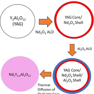
Powder atomic layer deposition process is used to coat nanopowders of host materials (e.g. yttrium aluminum garnet) with optically active neodymium organometal precursor followed by O2/O3 RF plasma to convert to a single layer of Nd2O3. The process can be repeated to build arbitrarily thick layers with custom doping profiles and followed by post-…

This invention proposes using a pulse laser configured to generate laser pulses and a controller for controlling operation of the pulse laser. The controller is further configured to control the pulse laser to cause the pulse laser to generate at least one of the laser pulses with a spatiotemporally varying laser fluence over a duration of at least one of the laser pulses. The spatiotemporally…


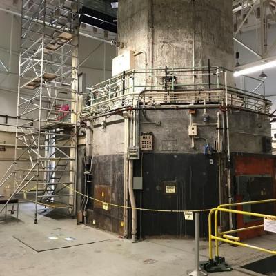
The new LLNL technique works by transiently removing and trapping concrete or rock surface material, so that contaminants are confined in a manner that is easy to isolate and remove. Our studies suggest that 10 m2 of surface could be processed per hour. The technique easily scales to more surface/hr.


