
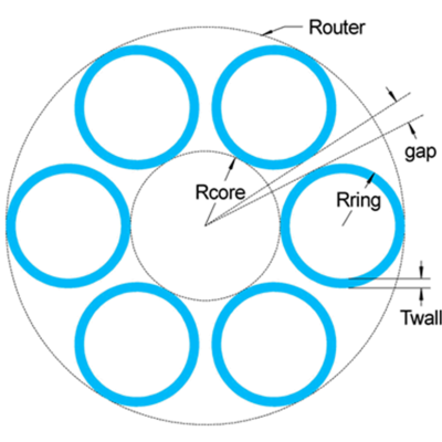
This LLNL invention proposes a new microstructured large mode area fiber design that enhances the confinement of the core mode while strongly suppressing thermal or scattering mediated dynamic couplings with higher order modes thought to be responsible for generating undesirable Transverse Mode Instabilities. The design accomplishes higher order mode suppression and core mode confinement by…
Image

For this method, a Silicon on Insulator (SOI) wafer is used to tailor etch rates and thickness in initial steps of the process. The simple three step process approach is comprised of grayscale lithography, deep reactive-ion etch (DRIE) and liftoff of the SOI wafer. The liftoff process is used to dissolve the insulating layer, thus separating sections of the wafer as individual…
Image

Livermore Lab's SBC grating optics benefit from the combination of the following key technologies:
- LLNL proprietary optical coating designs utilizing >100 thin film layers – enables ultra-low-loss, ppm transmission levels through the coating, high diffraction efficiency, and large bandwidth.
- LLNL proprietary dispersive surface relief structure…