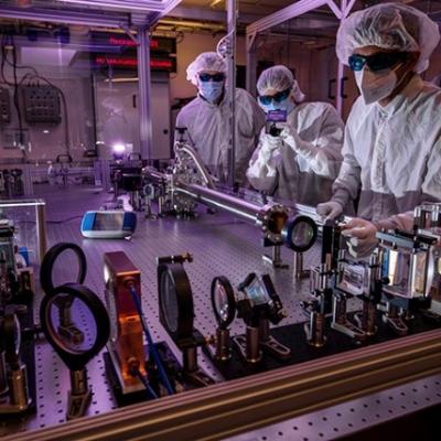
This invention proposes achieving the same effect of a single, high intensity pulse through the use of a closely spaced burst of short duration pulses. By keeping the intensity of the individual pulses below the damage threshold the risk of catastrophic damage is greatly mitigated. Additionally, the pulses are directed to strike the target at locations temporally and spatially sufficiently…
Keywords
- (-) Show all (240)
- Additive Manufacturing (55)
- Instrumentation (41)
- Synthesis and Processing (21)
- Sensors (14)
- Diagnostics (11)
- Imaging Systems (9)
- Photoconductive Semiconductor Switches (PCSS) (9)
- 3D Printing (8)
- Carbon Utilization (7)
- Electric Grid (7)
- Materials for Energy Products (7)
- Semiconductors (7)
- Substrate Engraved Meta-Surface (SEMS) (7)
- Therapeutics (7)
- Compact Space Telescopes (6)
- Brain Computer Interface (BCI) (5)
- Data Science (5)
- Diode Lasers (5)
- Optical Switches (5)
- Laser Materials Processing (4)
Technology Portfolios

This invention proposes the use of a nonlinear spectral broadening subsystem as a post-CPA pulse compression add-on for high energy laser systems. The proposed solution utilizes the beam profile of a high peak power laser as a reference to shape a highly transmissive nonlinear plastic (e.g., CR39) itself to ensure a spatially homogeneous nonlinear spectral broadening.

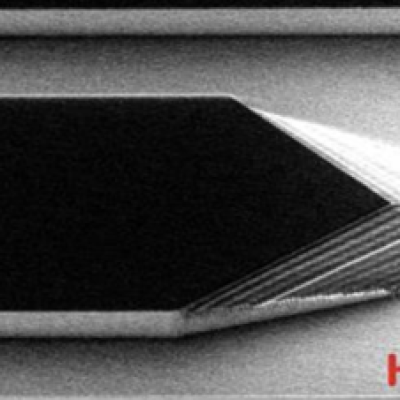
For this method, a Silicon on Insulator (SOI) wafer is used to tailor etch rates and thickness in initial steps of the process. The simple three step process approach is comprised of grayscale lithography, deep reactive-ion etch (DRIE) and liftoff of the SOI wafer. The liftoff process is used to dissolve the insulating layer, thus separating sections of the wafer as individual…


