
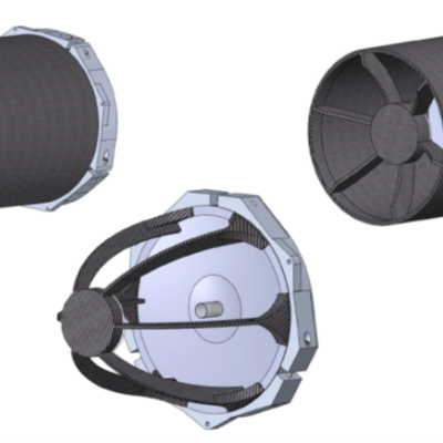
The approach is to use foundational materials science, structural design, thermal analysis, optic fabrication, and space systems engineering, and to use optimize them through large-scale simulation to realize meter-scale telescopes at 10X cost reduction. LLNL’s folded Gregorian design integrates all alignment sensitive components into one static monolithic system. Like solid-…
Image

For this method, a Silicon on Insulator (SOI) wafer is used to tailor etch rates and thickness in initial steps of the process. The simple three step process approach is comprised of grayscale lithography, deep reactive-ion etch (DRIE) and liftoff of the SOI wafer. The liftoff process is used to dissolve the insulating layer, thus separating sections of the wafer as individual…