
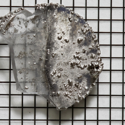
LLNL researchers have continued to develop their pioneering DIW 3D-printed glass optics technology that allows for the 3D printing of single- and multi-material optical glass compositions in complex shapes. This LLNL invention further proposes incorporating dopants (including, but not limited to TiO2 and Pd) into slurries and inks for 3D printing of glass components that can then be directly…
Image

For this method, a Silicon on Insulator (SOI) wafer is used to tailor etch rates and thickness in initial steps of the process. The simple three step process approach is comprised of grayscale lithography, deep reactive-ion etch (DRIE) and liftoff of the SOI wafer. The liftoff process is used to dissolve the insulating layer, thus separating sections of the wafer as individual…
Image

LLNL researchers have developed a custom resin formulation which uses a dispersing solvent and only a multifunctional monomer as the binding agent. The dispersing solvent system typically used has multiple components meant to achieve excellent dispersal of silica in order to create a flowable resin (rather than a paste). The dispersing agent has low vapor pressure, which allows the 3D printed…