
For this method, a Silicon on Insulator (SOI) wafer is used to tailor etch rates and thickness in initial steps of the process. The simple three step process approach is comprised of grayscale lithography, deep reactive-ion etch (DRIE) and liftoff of the SOI wafer. The liftoff process is used to dissolve the insulating layer, thus separating sections of the wafer as individual silicon…
Image
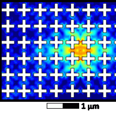
LLNL has developed a method of extending device lifetimes by imprinting into the device a shape that excludes specific vibrational modes, otherwise known as a phononic bandgap. Eliminating these modes prevents one of the primary energy loss pathways in these devices. LLNL’s new method enhances the coherence of superconducting circuits by introducing a phononic bandgap around the system’s…
Image
By combining 3D printing and dealloying., researchers at LLNL have developed a method for fabricating metal foams with engineered hierarchical architectures consisting of pores at least 3 distinct length scales. LLNL’s method uses direct ink writing (DIW), a 3D printing technique for additive manufacturing to fabricate hierarchical nanoporous metal foams with deterministically controlled 3D…
Image

LLNL has developed a compact and low-power cantilever-based sensor array, which has been used to detect various vapor-phase analytes. For further information on the latest developments, see the article "Sniffing the Air with an Electronic Nose."