
LLNL researchers has developed designs to augment WBG/UWBG-based OALVs to improve their power handling capability under CW operational environments. These designs include:
Image
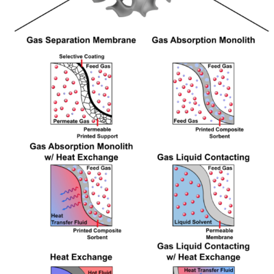
Hierarchical Triply Periodic Minimal Surface Structures For Efficient Two Fluid Flow Reactor Designs
LLNL researchers have devised a set of design principles that facilitates the development of practical TPMS-based two fluid flow reactors.; included in the design are these new concepts:
Image
![Filled (8,8) (left) and (15,15) (right) CNTs with [EMIM+][BF4- ] using SGTI with the proposed spliced soft-core potential (SSCP) approach](/sites/default/files/styles/scale_exact_400x400_/public/2023-10/Filled%20CNTs%20using%20SGTI.png?itok=Dy0ObN7i)
LLNL researchers have developed a novel simulation methodology using slow growth thermodynamic integration (SGTI) utilizing spliced soft-core interaction potential (SSCP). The approach to filling the molecular enclosures is a nonphysical one. Rather than filling the pores from the open ends this method creates steps in the algorithm that allow molecules to pass through the pore wall and…
Image

For this method, a Silicon on Insulator (SOI) wafer is used to tailor etch rates and thickness in initial steps of the process. The simple three step process approach is comprised of grayscale lithography, deep reactive-ion etch (DRIE) and liftoff of the SOI wafer. The liftoff process is used to dissolve the insulating layer, thus separating sections of the wafer as individual silicon…
Image

Design and construction of a photoconductive switch requires a diamond photoconductor illuminated by light of a certain excitation wavelength. The diamond material is specifically doped with substitutional nitrogen, which act as a source of electrons. The device architecture allows maximum light entering the aperture. The top and bottom electrodes are made of ultra wide band gap (UWBG)…
Image

The approach is to use a custom-designed frustrum and attach it to the optical fiber that connects to the PCSS. Light from the fiber enters the frustrum, spreads out, and enters the PCSS. Any unabsorbed light re-enters the frustrum and, because of its geometry, reflects back into the PCSS itself with only a negligible fraction escaping from the fiber. The shape of the novel frustrum is…
Image

By combining 3D printing and dealloying., researchers at LLNL have developed a method for fabricating metal foams with engineered hierarchical architectures consisting of pores at least 3 distinct length scales. LLNL’s method uses direct ink writing (DIW), a 3D printing technique for additive manufacturing to fabricate hierarchical nanoporous metal foams with deterministically controlled 3D…
Image

The Optical Transconductance Varistor (OTV, formerly Opticondistor) overcomes depletion region voltage limitations by optically exciting wide bandgap materials in a compact package. A 100μm thick crystal could have the capability approaching 40kV and would replace numerous equivalent junction devices. Thus, unlike present junction transistors or diodes, this wide bandgap device can be stacked…
Image

To overcome limitations with cellular silicone foams, LLNL innovators have developed a new 3D energy absorbing material with tailored/engineered bulk-scale properties. The energy absorbing material has 3D patterned architectures specially designed for specific energy absorbing properties. The combination of LLNL's capabilities in advanced modeling and simulation and the additive…
Image

LLNL has developed a compact and low-power cantilever-based sensor array, which has been used to detect various vapor-phase analytes. For further information on the latest developments, see the article "Sniffing the Air with an Electronic Nose."